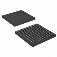
AT91SAM9R64-CU Atmel, AT91SAM9R64-CU Datasheet - Page 659

AT91SAM9R64-CU
Manufacturer Part Number
AT91SAM9R64-CU
Description
MCU ARM9 64K SRAM 144-LFBGA
Manufacturer
Atmel
Series
AT91SAMr
Specifications of AT91SAM9R64-CU
Core Processor
ARM9
Core Size
16/32-Bit
Speed
240MHz
Connectivity
EBI/EMI, I²C, MMC, SPI, SSC, UART/USART, USB
Peripherals
AC'97, POR, PWM, WDT
Number Of I /o
49
Program Memory Size
32KB (32K x 8)
Program Memory Type
ROM
Ram Size
72K x 8
Voltage - Supply (vcc/vdd)
1.08 V ~ 1.32 V
Data Converters
A/D 3x10b
Oscillator Type
Internal
Operating Temperature
-40°C ~ 85°C
Package / Case
144-LFBGA
Processor Series
AT91SAMx
Core
ARM926EJ-S
Data Bus Width
32 bit
Data Ram Size
64 KB
Interface Type
2-Wire, SPI, SSC, USART
Maximum Clock Frequency
240 MHz
Number Of Programmable I/os
118
Number Of Timers
4
Maximum Operating Temperature
+ 85 C
Mounting Style
SMD/SMT
3rd Party Development Tools
JTRACE-ARM-2M, MDK-ARM, RL-ARM, ULINK2
Development Tools By Supplier
AT91SAM-ICE, AT91-ISP, AT91SAM9RL-EK
Minimum Operating Temperature
- 40 C
On-chip Adc
10 bit, 3 Channel
Controller Family/series
AT91SAM9xxx
No. Of I/o's
49
Ram Memory Size
64KB
Cpu Speed
240MHz
No. Of Timers
3
Rohs Compliant
Yes
Package
144LFBGA
Device Core
ARM926EJ-S
Family Name
91S
Maximum Speed
240 MHz
Operating Supply Voltage
1.8|3.3 V
For Use With
AT91SAM-ICE - EMULATOR FOR AT91 ARM7/ARM9
Lead Free Status / RoHS Status
Lead free / RoHS Compliant
Eeprom Size
-
Lead Free Status / Rohs Status
Lead free / RoHS Compliant
Available stocks
Company
Part Number
Manufacturer
Quantity
Price
Part Number:
AT91SAM9R64-CU
Manufacturer:
ATMEL/爱特梅尔
Quantity:
20 000
- Current page: 659 of 903
- Download datasheet (13Mb)
6289C–ATARM–28-May-09
Table 39-8.
The duty cycles for gray levels 0 and 15 are 0 and 1, respectively.
The same DP_i register can be used for the pairs for which the sum of duty cycles is 1 (e.g., 1/7
and 6/7). The dithering pattern for the first pair member is the inversion of the one for the
second.
The DP_i registers contain a series of 4-bit patterns. The (3-m)
pixel with horizontal coordinate x = 4n + m (n is an integer and m ranges from 0 to 3) should be
turned on or off in the current frame. The operation is shown by the examples below.
Consider the pixels a, b, c and d with the horizontal coordinates 4*n+0, 4*n+1, 4*n+2 and 4*n+3,
respectively. The four pixels should be displayed in gray level 9 (duty cycle 3/5) so the register
used is DP3_5 =”1010 0101 1010 0101 1111”.
The output sequence obtained in the data output for monochrome mode is shown in
Table 39-9.
Consider now color display mode and two pixels p0 and p1 with the horizontal coordinates
4*n+0, and 4*n+1. A color pixel is composed of three components: {R, G, B}. Pixel p0 will be dis-
played sending the color components {R0, G0, B0} to the display. Pixel p1 will be displayed
sending the color components {R1, G1, B1}. Suppose that the data read from memory and
mapped to the lookup tables corresponds to shade level 10 for the three color components of
Gray Level
8
7
6
5
4
3
2
1
0
Frame
Number
N
N+1
N+2
N+3
N+4
N+5
N+6
N+7
...
Dithering Duty Cycle
Dithering Algorithm for Monochrome Mode
Pattern
1010
0101
1010
0101
1111
1010
0101
1010
...
AT91SAM9R64/RL64 Preliminary
Duty Cycle
4/7
1/2
3/7
2/5
1/3
1/4
1/5
1/7
0
ON
OFF
ON
OFF
ON
ON
OFF
ON
...
Pixel a
Pixel b
OFF
ON
OFF
ON
ON
OFF
ON
OFF
...
th
bit of the pattern determines if a
Pattern Register
DP4_7
~DP1_2
~DP4_7
~DP3_5
~DP2_3
~DP3_4
~DP4_5
~DP6_7
-
Pixel c
ON
OFF
ON
OFF
ON
ON
OFF
ON
...
Pixel d
OFF
ON
OFF
ON
ON
OFF
ON
OFF
...
Table
39-9.
659
Related parts for AT91SAM9R64-CU
Image
Part Number
Description
Manufacturer
Datasheet
Request
R

Part Number:
Description:
MCU, MPU & DSP Development Tools KICKSTART KIT FOR AT91SAM9 PLUS
Manufacturer:
IAR Systems

Part Number:
Description:
DEV KIT FOR AVR/AVR32
Manufacturer:
Atmel
Datasheet:

Part Number:
Description:
INTERVAL AND WIPE/WASH WIPER CONTROL IC WITH DELAY
Manufacturer:
ATMEL Corporation
Datasheet:

Part Number:
Description:
Low-Voltage Voice-Switched IC for Hands-Free Operation
Manufacturer:
ATMEL Corporation
Datasheet:

Part Number:
Description:
MONOLITHIC INTEGRATED FEATUREPHONE CIRCUIT
Manufacturer:
ATMEL Corporation
Datasheet:

Part Number:
Description:
AM-FM Receiver IC U4255BM-M
Manufacturer:
ATMEL Corporation
Datasheet:

Part Number:
Description:
Monolithic Integrated Feature Phone Circuit
Manufacturer:
ATMEL Corporation
Datasheet:

Part Number:
Description:
Multistandard Video-IF and Quasi Parallel Sound Processing
Manufacturer:
ATMEL Corporation
Datasheet:

Part Number:
Description:
High-performance EE PLD
Manufacturer:
ATMEL Corporation
Datasheet:

Part Number:
Description:
8-bit Flash Microcontroller
Manufacturer:
ATMEL Corporation
Datasheet:

Part Number:
Description:
2-Wire Serial EEPROM
Manufacturer:
ATMEL Corporation
Datasheet:


