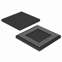
LPC3130FET180,551 NXP Semiconductors, LPC3130FET180,551 Datasheet - Page 34

LPC3130FET180,551
Manufacturer Part Number
LPC3130FET180,551
Description
IC ARM9 MCU 180MHZ 180-TFBGA
Manufacturer
NXP Semiconductors
Series
LPC3000r
Datasheet
1.OM11024.pdf
(72 pages)
Specifications of LPC3130FET180,551
Package / Case
180-TFBGA
Core Processor
ARM9
Core Size
32-Bit
Speed
180MHz
Connectivity
EBI/EMI, I²C, MMC, SPI, UART/USART, USB OTG
Peripherals
DMA, I²S, LCD, PWM, WDT
Program Memory Type
ROMless
Ram Size
96K x 8
Voltage - Supply (vcc/vdd)
1.1 V ~ 3.6 V
Data Converters
A/D 4x10b
Oscillator Type
External
Operating Temperature
-40°C ~ 85°C
Processor Series
LPC31
Core
ARM926EJ-S
Data Bus Width
16 bit, 32 bit
Data Ram Size
96 KB
Interface Type
I2C/I2S/UART/USB
Maximum Clock Frequency
180 MHz
Number Of Timers
4
Operating Supply Voltage
2.7 V to 3.6 V
Maximum Operating Temperature
+ 85 C
Mounting Style
SMD/SMT
3rd Party Development Tools
MDK-ARM, RL-ARM, ULINK2
Minimum Operating Temperature
- 40 C
On-chip Adc
4-ch x 10-bit
Cpu Family
LPC3000
Device Core
ARM926EJ-S
Device Core Size
16/32Bit
Frequency (max)
180MHz
Program Memory Size
Not Required
Total Internal Ram Size
96KB
Number Of Timers - General Purpose
4
Operating Supply Voltage (typ)
1.2/1.8/2.8/3.3/5V
Operating Supply Voltage (max)
1.3/3.6V
Operating Supply Voltage (min)
1/1.1/1.65/2.7V
Instruction Set Architecture
RISC
Operating Temp Range
-40C to 85C
Operating Temperature Classification
Industrial
Mounting
Surface Mount
Pin Count
180
Package Type
TFBGA
Package
180TFBGA
Family Name
LPC3000
Maximum Speed
180 MHz
Lead Free Status / RoHS Status
Lead free / RoHS Compliant
For Use With
568-4850 - KIT EVAL FOR LPC313X568-4062 - DEBUGGER J-LINK JTAG568-4061 - DEBUGGER U-LINK2 JTAG FOR NXP
Number Of I /o
-
Eeprom Size
-
Program Memory Size
-
Lead Free Status / Rohs Status
Lead free / RoHS Compliant
Other names
568-4696
935288013551
LPC3130FET180-S
935288013551
LPC3130FET180-S
Available stocks
Company
Part Number
Manufacturer
Quantity
Price
Company:
Part Number:
LPC3130FET180,551
Manufacturer:
NXP Semiconductors
Quantity:
10 000
NXP Semiconductors
LPC3130_3131
Preliminary data sheet
6.26.3 Supply domains
6.27 Timer module
6.28 Pulse Width Modulation (PWM) module
The EBI unit between the NAND flash interface and the MPMC contains an arbiter that
determines which interface is muxed to the outside world. Both NAND flash and
SDRAM/SRAM initiate a request to the EBI unit. This request is granted using round-robin
arbitration (see
As is shown in
different supply domain than the LCD interface. The EBI control and address signals are
muxed with the LCD interface signals and are part of supply domain SUP8. The
SDRAM/SRAM data lines are shared with the NAND flash through the EBI and are part of
supply domain SUP4. Therefore the following rules apply for connecting memories:
The LPC3130/3131 contains four fully independent timer modules, which can be used to
generate interrupts after a pre-set time interval has elapsed.
This module has the following features:
This PWM can be used to generate a pulse width modulated or a pulse density modulated
signal. With an external low pass filter, the module can be used to generate a
low-frequency analog signal. A typical use of the output of the module is to control the
backlight of an LCD display.
This module has the following features:
1. SDRAM and bus-based LCD or SRAM: This is the MPMC mode. The supply voltage
2. Dedicated LCD interface only: This is the LCD mode. The NAND flash supply voltage
•
•
•
•
•
•
for SDRAM/SRAM/bus-based LCD and NAND flash must be the same.The dedicated
LCD interface is not available in this MPMC mode.
(SUP4) can be different from the LCD supply voltage (SUP8).
Each timer is a 32 bit wide down-counter with selectable pre-scale. The pre-scaler
allows using either the module clock directly or the clock divided by 16 or 256.
Two modes of operation:
– Free-running timer: The timer generates an interrupt when the counter reaches
– Periodic timer: The timer generates an interrupt when the counter reaches zero. It
At any time the current timer value can be read.
At any time the value in the load register may be re-written, causing the timer to
restart.
Supports Pulse Width Modulation (PWM) with software controlled duty cycle.
Supports Pulse Density Modulation (PDM) with software controlled pulse density.
zero. The timer wraps around to 0xFFFFFFFF and continues counting down.
reloads the value from a load register and continues counting down from that
value. An interrupt will be generated every time the counter reaches zero. This
effectively gives a repeated interrupt at a regular interval.
Figure 9
All information provided in this document is subject to legal disclaimers.
Section
Rev. 1.04 — 27 May 2010
6.6).
the EBI (NAND flash/MPMC-control/data) is connected to a
Low-cost, low-power ARM926EJ-S microcontrollers
LPC3130/3131
© NXP B.V. 2010. All rights reserved.
34 of 72


