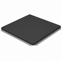
LPC2478FBD208,551 NXP Semiconductors, LPC2478FBD208,551 Datasheet - Page 46

LPC2478FBD208,551
Manufacturer Part Number
LPC2478FBD208,551
Description
IC ARM7 MCU 512K LCD 208-LQFP
Manufacturer
NXP Semiconductors
Series
LPC2400r
Datasheets
1.OM11077.pdf
(91 pages)
2.OM11077.pdf
(792 pages)
3.OM11077.pdf
(10 pages)
4.LPC2478FBD208551.pdf
(89 pages)
Specifications of LPC2478FBD208,551
Program Memory Type
FLASH
Program Memory Size
512KB (512K x 8)
Package / Case
208-LQFP
Core Processor
ARM7
Core Size
16/32-Bit
Speed
72MHz
Connectivity
CAN, EBI/EMI, Ethernet, I²C, Microwire, MMC, SPI, SSI, SSP, UART/USART, USB OTG
Peripherals
Brown-out Detect/Reset, DMA, I²S, LCD, POR, PWM, WDT
Number Of I /o
160
Ram Size
96K x 8
Voltage - Supply (vcc/vdd)
3 V ~ 3.6 V
Data Converters
A/D 8x10b; D/A 1x10b
Oscillator Type
Internal
Operating Temperature
-40°C ~ 85°C
Processor Series
LPC24
Core
ARM7TDMI-S
Data Bus Width
16 bit, 32 bit
Data Ram Size
98 KB
Interface Type
CAN/I2C/I2S/IrDA/SPI/SSP/UART/USB
Maximum Clock Frequency
72 MHz
Number Of Programmable I/os
160
Number Of Timers
4
Operating Supply Voltage
3.3 V
Maximum Operating Temperature
+ 85 C
Mounting Style
SMD/SMT
3rd Party Development Tools
MDK-ARM, RL-ARM, ULINK2, DK-35TS-LPC2478, DK-57TS-LPC2478, DK-57VTS-LPC2478, SOMDIMM-LPC2478, SAB-TFBGA208, KSK-LPC2478-JL, MCB2470
Development Tools By Supplier
OM11015, OM11019, OM11022
Minimum Operating Temperature
- 40 C
On-chip Adc
8-ch x 10-bit
On-chip Dac
1-ch x 10-bit
Lead Free Status / RoHS Status
Lead free / RoHS Compliant
For Use With
622-1034 - PROGRAMMERS, DEVELOPMENT SYSTEMS622-1033 - KIT LCD TOUCH 5.7" FOR LPC2478MCB2470 - BOARD EVAL NXP LPC247X SERIESOM11022 - EVAL LPC-STICK WITH LPC2478OM11019 - BOARD EVAL FOR LPC2478568-4742 - MODULE DIMM LPC2478 ARM7568-4741 - KIT LCD TOUCH 5.7" FOR LPC2478622-1028 - KIT LCD TOUCH 5.7" FOR LPC2478KSDKLPC2478-PL - KIT IAR KICKSTART NXP LPC2478622-1024 - BOARD SCKT ADAPTER FOR TFBGA208568-4369 - BOARD EVAL FOR LPC2478622-1005 - USB IN-CIRCUIT PROG ARM7 LPC2K
Eeprom Size
-
Lead Free Status / Rohs Status
Lead free / RoHS Compliant
Other names
568-4363
935284069551
LPC2478FBD208-S
935284069551
LPC2478FBD208-S
Available stocks
Company
Part Number
Manufacturer
Quantity
Price
Company:
Part Number:
LPC2478FBD208,551
Manufacturer:
NXP Semiconductors
Quantity:
10 000
Part Number:
LPC2478FBD208,551
Manufacturer:
NXP/恩智浦
Quantity:
20 000
NXP Semiconductors
LPC2470
Product data sheet
7.26.2 Boot process
7.26.3 Brownout detection
7.26.4 AHB
level, starts the wake-up timer (see description in
causing reset to remain asserted until the external Reset is de-asserted, the oscillator is
running, and a fixed number of clocks have passed.
Once the internal reset is removed, all of the processor and peripheral registers have
been initialized to predetermined values and the LPC2470 continues with booting from an
external static memory.
The processor always boots from the off-chip static memory bank 1, executing code from
address 0x8100 0000 (see
boot process initiated by POR, the boot pins P3[15]/D15 and P3[14]/D14 are sampled,
and the external memory banks 0 and 1 are configured with the same data bus width. The
data bus width is determined by the setting of the two boot pins. Unused address pins are
configured as GPIO. See
address and data bus interface details.
Remark: After POR, the address ranges of chip select 1 and chip select 0 are swapped.
The user code residing in the external boot memory must be linked to execute from
address location 0x8000 0000.
When booting from external memory, the interrupt vectors are mapped to the bottom of
the external memory. Once booting is over, the application must map interrupt vectors to
the proper domain.
The LPC2470 includes 2-stage monitoring of the voltage on the V
voltage falls below 2.95 V, the BOD asserts an interrupt signal to the Vectored Interrupt
Controller. This signal can be enabled for interrupt in the Interrupt Enable Register in the
VIC in order to cause a CPU interrupt; if not, software can monitor the signal by reading a
dedicated status register.
The second stage of low-voltage detection asserts a BOD Reset and generates a Reset (if
this reset source is enabled in software) to inactivate the LPC2470 when the voltage on
the V
below 1 V, at which point the power-on reset circuitry maintains the overall Reset.
Both the 2.95 V and 2.65 V thresholds include some hysteresis. In normal operation, this
hysteresis allows the 2.95 V detection to reliably interrupt, or a regularly-executed event
loop to sense the condition.
The LPC2470 implements two AHB in order to allow the Ethernet block to operate without
interference caused by other system activity. The primary AHB, referred to as AHB1,
includes the Vectored Interrupt Controller, GPDMA controller, USB interface, and 16 kB
SRAM.
The second AHB, referred to as AHB2, includes only the Ethernet block and an
associated 16 kB SRAM. In addition, a bus bridge is provided that allows the secondary
AHB to be a bus master on AHB1, allowing expansion of Ethernet buffer space into
off-chip memory or unused space in memory residing on AHB1.
DD(DCDC)(3V3)
All information provided in this document is subject to legal disclaimers.
pins falls below 2.65 V. The BOD circuit maintains this reset down
Rev. 3 — 14 February 2011
Section 14.2 “Suggested boot memory interface solutions”
Table 5 “LPC2470 memory usage and
Flashless 16-bit/32-bit microcontroller
Section 7.25.3 “Wake-up
DD(DCDC)(3V3)
details”). During the
LPC2470
© NXP B.V. 2011. All rights reserved.
timer”),
pins. If this
46 of 89
for


