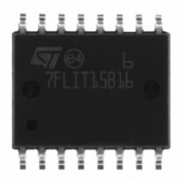
ST7FLIT15BY1M6 STMicroelectronics, ST7FLIT15BY1M6 Datasheet - Page 74

ST7FLIT15BY1M6
Manufacturer Part Number
ST7FLIT15BY1M6
Description
IC MCU 8BIT 4K FLASH 16-SOIC
Manufacturer
STMicroelectronics
Series
ST7r
Datasheet
1.ST7FLIT15BY1M6.pdf
(159 pages)
Specifications of ST7FLIT15BY1M6
Core Processor
ST7
Core Size
8-Bit
Speed
8MHz
Connectivity
SPI
Peripherals
LVD, POR, PWM, WDT
Number Of I /o
11
Program Memory Size
4KB (4K x 8)
Program Memory Type
FLASH
Ram Size
256 x 8
Voltage - Supply (vcc/vdd)
2.7 V ~ 5.5 V
Data Converters
A/D 7x10b
Oscillator Type
Internal
Operating Temperature
-40°C ~ 85°C
Package / Case
16-SOIC (0.300", 7.5mm Width)
Controller Family/series
ST7
No. Of I/o's
13
Ram Memory Size
256Byte
Cpu Speed
8MHz
No. Of Timers
5
Rohs Compliant
Yes
Processor Series
ST7FLIT1x
Core
ST7
Data Bus Width
8 bit
Data Ram Size
256 B
Interface Type
SPI
Maximum Clock Frequency
8 MHz
Number Of Programmable I/os
17
Number Of Timers
4
Maximum Operating Temperature
+ 85 C
Mounting Style
SMD/SMT
Development Tools By Supplier
ST7FLITE-SK/RAIS, ST7MDT10-DVP3, ST7MDT10-EMU3, STX-RLINK
Minimum Operating Temperature
- 40 C
On-chip Adc
10 bit, 7 Channel
For Use With
497-5049 - KIT STARTER RAISONANCE ST7FLITE497-5046 - KIT TOOL FOR ST7/UPSD/STR7 MCU
Lead Free Status / RoHS Status
Lead free / RoHS Compliant
Eeprom Size
-
Lead Free Status / Rohs Status
Details
Other names
497-8245-5
ST7FLIT15BY1M6
ST7FLIT15BY1M6
Available stocks
Company
Part Number
Manufacturer
Quantity
Price
ST7LITE1xB
DUAL 12-BIT AUTORELOAD TIMER 4 (Cont’d)
BREAK CONTROL REGISTER (BREAKCR)
Read/Write
Reset Value: 0000 0000 (00h)
Bit 7 = BRSEL Break Input Selection
This bit is read/write by software and cleared by
hardware after reset. It selects the active Break
signal from external BREAK pin and the output of
the comparator.
0: External BREAK pin is selected for break mode.
1: Comparator output is selected for break mode.
Bit 6 = BREDGE Break Input Edge Selection
This bit is read/write by software and cleared by
hardware after reset. It selects the active level of
Break signal.
0: Low level of Break selected as active level.
1: High level of Break selected as active level.
Bit 5 = BA Break Active.
This bit is read/write by software, cleared by hard-
ware after reset and set by hardware when the ac-
tive level defined by the BREDGE bit is applied on
the BREAK pin. It activates/deactivates the Break
function.
0: Break not active
1: Break active
Bit 4 = BPEN Break Pin Enable.
This bit is read/write by software and cleared by
hardware after Reset.
0: Break pin disabled
1: Break pin enabled
Bits 3:0 = PWM[3:0] Break Pattern.
These bits are read/write by software and cleared
by hardware after a reset. They are used to force
the four PWMx output signals into a stable state
when the Break function is active and correspond-
ing OEx bit is set.
74/159
1
BRSEL BREDGE
7
BA
BPEN
PWM3 PWM2 PWM1 PWM0
0
PWMx DUTY CYCLE REGISTER HIGH (DCRxH)
Read / Write
Reset Value: 0000 0000 (00h)
Bits 15:12 = Reserved.
PWMx DUTY CYCLE REGISTER LOW (DCRxL)
Read / Write
Reset Value: 0000 0000 (00h)
Bits 11:0 = DCRx[11:0] PWMx Duty Cycle Value
This 12-bit value is written by software. It defines
the duty cycle of the corresponding PWM output
signal (see
In PWM mode (OEx=1 in the PWMCR register)
the DCR[11:0] bits define the duty cycle of the
PWMx output signal (see
Compare mode, they define the value to be com-
pared with the 12-bit upcounter value.
INPUT CAPTURE REGISTER HIGH (ATICRH)
Read only
Reset Value: 0000 0000 (00h)
Bits 15:12 = Reserved.
INPUT CAPTURE REGISTER LOW (ATICRL)
Read only
Reset Value: 0000 0000 (00h)
DCR7 DCR6 DCR5 DCR4 DCR3 DCR2 DCR1 DCR0
ICR7
15
15
0
7
0
7
ICR6
0
0
Figure
ICR5
0
0
4).
ICR4
0
0
DCR11 DCR10 DCR9 DCR8
ICR11 ICR10
ICR3
Figure
ICR2
4). In Output
ICR9
ICR1
ICR8
ICR0
8
8
0
0


