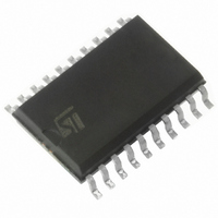
ST7FLITE19F1M6 STMicroelectronics, ST7FLITE19F1M6 Datasheet - Page 49

ST7FLITE19F1M6
Manufacturer Part Number
ST7FLITE19F1M6
Description
IC MCU 8BIT 4K 20-SOIC
Manufacturer
STMicroelectronics
Series
ST7r
Datasheet
1.ST7FLITE15F1M6.pdf
(131 pages)
Specifications of ST7FLITE19F1M6
Core Processor
ST7
Core Size
8-Bit
Speed
8MHz
Connectivity
SPI
Peripherals
LVD, POR, PWM, WDT
Number Of I /o
15
Program Memory Size
4KB (4K x 8)
Program Memory Type
FLASH
Eeprom Size
128 x 8
Ram Size
256 x 8
Voltage - Supply (vcc/vdd)
2.4 V ~ 5.5 V
Data Converters
A/D 7x10b
Oscillator Type
Internal
Operating Temperature
-40°C ~ 85°C
Package / Case
20-SOIC (7.5mm Width)
Processor Series
ST7FLITE1x
Core
ST7
Data Bus Width
8 bit
Data Ram Size
256 B
Interface Type
SPI
Maximum Clock Frequency
8 MHz
Number Of Programmable I/os
15
Number Of Timers
1 x 12 bit / 2 x 8 bit
Operating Supply Voltage
2.4 V to 5.5 V
Maximum Operating Temperature
+ 85 C
Mounting Style
SMD/SMT
Development Tools By Supplier
ST7FLIT2-COS/COM, ST7FLITE-SK/RAIS, ST7MDT10-DVP3, ST7MDT10-EMU3, STX-RLINK
Minimum Operating Temperature
- 40 C
On-chip Adc
7 bit x 10 bit
For Use With
497-5858 - EVAL BOARD PLAYBACK ST7FLITE497-5049 - KIT STARTER RAISONANCE ST7FLITE497-5046 - KIT TOOL FOR ST7/UPSD/STR7 MCU
Lead Free Status / RoHS Status
Contains lead / RoHS non-compliant
Other names
497-2133-5
Available stocks
Company
Part Number
Manufacturer
Quantity
Price
I/O PORTS (Cont’d)
Analog alternate function
Configure the I/O as floating input to use an ADC
input. The analog multiplexer (controlled by the
ADC registers) switches the analog voltage
present on the selected pin to the common analog
rail, connected to the ADC input.
Analog Recommendations
Do not change the voltage level or loading on any
I/O while conversion is in progress. Do not have
clocking pins located close to a selected analog
pin.
WARNING: The analog input voltage level must
be within the limits stated in the absolute maxi-
mum ratings.
10.3 I/O PORT IMPLEMENTATION
The hardware implementation on each I/O port de-
pends on the settings in the DDR and OR registers
and specific I/O port features such as ADC input or
open drain.
Switching these I/O ports from one state to anoth-
er should be done in a sequence that prevents un-
wanted side effects. Recommended safe transi-
tions are illustrated in
are potentially risky and should be avoided, since
they may present unwanted side-effects such as
spurious interrupt generation.
Figure
31. Other transitions
Figure 31. Interrupt I/O Port State Transitions
10.4 UNUSED I/O PINS
Unused I/O pins must be connected to fixed volt-
age levels. Refer to
10.5 LOW POWER MODES
10.6 INTERRUPTS
The external interrupt event generates an interrupt
if the corresponding configuration is selected with
DDR and OR registers and if the I bit in the CC
register is cleared (RIM instruction).
floating/pull-up
WAIT
HALT
External interrupt on
selected external
event
Mode
Interrupt Event
interrupt
INPUT
01
No effect on I/O ports. External interrupts
cause the device to exit from WAIT mode.
No effect on I/O ports. External interrupts
cause the device to exit from HALT mode.
(reset state)
floating
INPUT
00
Section
Event
Flag
-
Description
open-drain
Control
OUTPUT
Enable
DDRx
13.8.
ORx
Bit
10
XX
= DDR, OR
from
Wait
Exit
Yes
ST7LITE1
OUTPUT
push-pull
11
49/131
from
Exit
Halt
Yes
1


