STM32F102C4T6A STMicroelectronics, STM32F102C4T6A Datasheet - Page 6
STM32F102C4T6A
Manufacturer Part Number
STM32F102C4T6A
Description
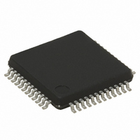
MCU ARM 32BIT 16KB FLASH 48-LQFP
Manufacturer
STMicroelectronics
Series
STM32r
Datasheet
1.STM32F102C6T6A.pdf
(69 pages)
Specifications of STM32F102C4T6A
Core Processor
ARM® Cortex-M3™
Core Size
32-Bit
Speed
48MHz
Connectivity
I²C, IrDA, LIN, SPI, UART/USART, USB
Peripherals
DMA, PDR, POR, PVD, PWM, Temp Sensor, WDT
Number Of I /o
37
Program Memory Size
16KB (16K x 8)
Program Memory Type
FLASH
Ram Size
4K x 8
Voltage - Supply (vcc/vdd)
2 V ~ 3.6 V
Data Converters
A/D 10x12b
Oscillator Type
Internal
Operating Temperature
-40°C ~ 85°C
Package / Case
48-LQFP
For Use With
497-10030 - STARTER KIT FOR STM32497-8853 - BOARD DEMO STM32 UNIV USB-UUSCIKSDKSTM32-PL - KIT IAR KICKSTART STM32 CORTEXM3497-8512 - KIT STARTER FOR STM32F10XE MCU497-8505 - KIT STARTER FOR STM32F10XE MCU497-8304 - KIT STM32 MOTOR DRIVER BLDC497-6438 - BOARD EVALUTION FOR STM32 512K497-6289 - KIT PERFORMANCE STICK FOR STM32MCBSTM32UME - BOARD EVAL MCBSTM32 + ULINK-MEMCBSTM32U - BOARD EVAL MCBSTM32 + ULINK2497-6053 - KIT STARTER FOR STM32497-6052 - KIT STARTER FOR STM32497-6050 - KIT STARTER FOR STM32497-6049 - KIT EVALUATION LOW COST STM32497-6048 - BOARD EVALUATION FOR STM32497-6047 - KIT DEVELOPMENT FOR STM32497-5046 - KIT TOOL FOR ST7/UPSD/STR7 MCU
Lead Free Status / RoHS Status
Lead free / RoHS Compliant
Eeprom Size
-
Lead Free Status / Rohs Status
Details
Other names
497-8305
Available stocks
Company
Part Number
Manufacturer
Quantity
Price
Company:

Part Number:
STM32F102C4T6A
Manufacturer:
STMicroelectronics
Quantity:
10 000
Company:
Part Number:
STM32F102C4T6ATR
Manufacturer:
STMicroelectronics
Quantity:
10 000


List of figures
List of figures
Figure 1.
Figure 2.
Figure 3.
Figure 4.
Figure 5.
Figure 6.
Figure 7.
Figure 8.
Figure 9.
Figure 10.
Figure 11.
Figure 12.
Figure 13.
Figure 14.
Figure 15.
Figure 16.
Figure 17.
Figure 18.
Figure 19.
Figure 20.
Figure 21.
Figure 22.
Figure 23.
Figure 24.
Figure 25.
Figure 26.
Figure 27.
Figure 28.
Figure 29.
Figure 30.
Figure 31.
Figure 32.
Figure 33.
Figure 34.
6/69
STM32F102xx low-density USB access line block diagram . . . . . . . . . . . . . . . . . . . . . . . . 10
Clock tree . . . . . . . . . . . . . . . . . . . . . . . . . . . . . . . . . . . . . . . . . . . . . . . . . . . . . . . . . . . . . . 11
STM32F102xx low-density USB access line LQFP48 pinout . . . . . . . . . . . . . . . . . . . . . . . 18
STM32F102xx low-density USB access line LQFP64 pinout . . . . . . . . . . . . . . . . . . . . . . . 18
Memory map . . . . . . . . . . . . . . . . . . . . . . . . . . . . . . . . . . . . . . . . . . . . . . . . . . . . . . . . . . . . 22
Pin loading conditions . . . . . . . . . . . . . . . . . . . . . . . . . . . . . . . . . . . . . . . . . . . . . . . . . . . . . 24
Pin input voltage . . . . . . . . . . . . . . . . . . . . . . . . . . . . . . . . . . . . . . . . . . . . . . . . . . . . . . . . . 24
Power supply scheme. . . . . . . . . . . . . . . . . . . . . . . . . . . . . . . . . . . . . . . . . . . . . . . . . . . . . 24
Current consumption measurement scheme . . . . . . . . . . . . . . . . . . . . . . . . . . . . . . . . . . . 25
Typical current consumption in Run mode versus temperature (at 3.6 V) -
code with data processing running from RAM, peripherals enabled. . . . . . . . . . . . . . . . . . 31
Typical current consumption in Run mode versus temperature (at 3.6 V) -
code with data processing running from RAM, peripherals disabled . . . . . . . . . . . . . . . . . 31
Typical current consumption on V
V
Typical current consumption in Stop mode with regulator in Run mode versus
temperature at V
Typical current consumption in Stop mode with regulator in Low-power mode versus
temperature at V
Typical current consumption in Standby mode versus temperature at V
3.6 V . . . . . . . . . . . . . . . . . . . . . . . . . . . . . . . . . . . . . . . . . . . . . . . . . . . . . . . . . . . . . . . . . . 34
High-speed external clock source AC timing diagram . . . . . . . . . . . . . . . . . . . . . . . . . . . . 39
Low-speed external clock source AC timing diagram . . . . . . . . . . . . . . . . . . . . . . . . . . . . . 39
Typical application with an 8 MHz crystal . . . . . . . . . . . . . . . . . . . . . . . . . . . . . . . . . . . . . . 41
Typical application with a 32.768 kHz crystal . . . . . . . . . . . . . . . . . . . . . . . . . . . . . . . . . . . 42
I/O AC characteristics definition . . . . . . . . . . . . . . . . . . . . . . . . . . . . . . . . . . . . . . . . . . . . . 50
Recommended NRST pin protection . . . . . . . . . . . . . . . . . . . . . . . . . . . . . . . . . . . . . . . . . 50
I
SPI timing diagram - slave mode and CPHA=0 . . . . . . . . . . . . . . . . . . . . . . . . . . . . . . . . . 55
SPI timing diagram - slave mode and CPHA=1
SPI timing diagram - master mode
USB timings: definition of data signal rise and fall time . . . . . . . . . . . . . . . . . . . . . . . . . . . 57
ADC accuracy characteristics . . . . . . . . . . . . . . . . . . . . . . . . . . . . . . . . . . . . . . . . . . . . . . . 60
Typical connection diagram using the ADC . . . . . . . . . . . . . . . . . . . . . . . . . . . . . . . . . . . . 60
Power supply and reference decoupling. . . . . . . . . . . . . . . . . . . . . . . . . . . . . . . . . . . . . . . 61
LQFP64 – 10 x 10 mm, 64 pin low-profile quad flat package outline . . . . . . . . . . . . . . . . . 63
Recommended footprint
LQFP48 – 7 x 7 mm, 48-pin low-profile quad flat package outline . . . . . . . . . . . . . . . . . . . 64
Recommended footprint
LQFP64 P
2
BAT
C bus AC waveforms and measurement circuit
values . . . . . . . . . . . . . . . . . . . . . . . . . . . . . . . . . . . . . . . . . . . . . . . . . . . . . . . . . . . . 33
D
max vs. T
DD
DD
= 3.3 V and 3.6 V . . . . . . . . . . . . . . . . . . . . . . . . . . . . . . . . . . . . . . . . 33
= 3.3 V and 3.6 V . . . . . . . . . . . . . . . . . . . . . . . . . . . . . . . . . . . . . . . . 34
A
(1)
(1)
. . . . . . . . . . . . . . . . . . . . . . . . . . . . . . . . . . . . . . . . . . . . . . . . . . . 66
. . . . . . . . . . . . . . . . . . . . . . . . . . . . . . . . . . . . . . . . . . . . . . . . . 63
. . . . . . . . . . . . . . . . . . . . . . . . . . . . . . . . . . . . . . . . . . . . . . . . . 64
Doc ID 15057 Rev 3
BAT
(1)
. . . . . . . . . . . . . . . . . . . . . . . . . . . . . . . . . . . . . . . . . 56
with RTC on versus temperature at different
(1)
(1)
. . . . . . . . . . . . . . . . . . . . . . . . . . . . . . . 55
. . . . . . . . . . . . . . . . . . . . . . . . . . . . . . 53
STM32F102x4, STM32F102x6
DD
= 3.3 V and
Related parts for STM32F102C4T6A
Image
Part Number
Description
Manufacturer
Datasheet
Request
R

Part Number:
Description:
STMicroelectronics [RIPPLE-CARRY BINARY COUNTER/DIVIDERS]
Manufacturer:
STMicroelectronics
Datasheet:
Part Number:
Description:
STMicroelectronics [LIQUID-CRYSTAL DISPLAY DRIVERS]
Manufacturer:
STMicroelectronics
Datasheet:

Part Number:
Description:
BOARD EVAL FOR MEMS SENSORS
Manufacturer:
STMicroelectronics
Datasheet:
Part Number:
Description:
NPN TRANSISTOR POWER MODULE
Manufacturer:
STMicroelectronics
Datasheet:
Part Number:
Description:
TURBOSWITCH ULTRA-FAST HIGH VOLTAGE DIODE
Manufacturer:
STMicroelectronics
Datasheet:
Part Number:
Description:
Manufacturer:
STMicroelectronics
Datasheet:
Part Number:
Description:
DIODE / SCR MODULE
Manufacturer:
STMicroelectronics
Datasheet:
Part Number:
Description:
DIODE / SCR MODULE
Manufacturer:
STMicroelectronics
Datasheet:
Part Number:
Description:
Search -----> STE16N100
Manufacturer:
STMicroelectronics
Datasheet:
Part Number:
Description:
Search ---> STE53NA50
Manufacturer:
STMicroelectronics
Datasheet:
Part Number:
Description:
NPN Transistor Power Module
Manufacturer:
STMicroelectronics
Datasheet:
Part Number:
Description:
DIODE / SCR MODULE
Manufacturer:
STMicroelectronics
Datasheet: