M37544G2AGP#U0 Renesas Electronics America, M37544G2AGP#U0 Datasheet - Page 21
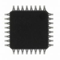
M37544G2AGP#U0
Manufacturer Part Number
M37544G2AGP#U0
Description
IC 740 MCU OTP 8K 32LQFP
Manufacturer
Renesas Electronics America
Series
740/38000r
Specifications of M37544G2AGP#U0
Core Processor
740
Core Size
8-Bit
Speed
8MHz
Connectivity
SIO, UART/USART
Peripherals
WDT
Number Of I /o
25
Program Memory Size
8KB (8K x 8)
Program Memory Type
QzROM
Ram Size
256 x 8
Voltage - Supply (vcc/vdd)
4 V ~ 5.5 V
Data Converters
A/D 6x8b
Oscillator Type
Internal
Operating Temperature
-20°C ~ 85°C
Package / Case
32-LQFP
Lead Free Status / RoHS Status
Lead free / RoHS Compliant
Eeprom Size
-
Available stocks
Company
Part Number
Manufacturer
Quantity
Price


Rev.1.04
REJ03B0012-0104Z
7544 Group
Interrupts
Interrupts occur by 12 different sources : 5 external sources, 6 in-
ternal sources and 1 software source.
Interrupt control
All interrupts except the BRK instruction interrupt have an interrupt
request bit and an interrupt enable bit, and they are controlled by
the interrupt disable flag. When the interrupt enable bit and the in-
terrupt request bit are set to “1” and the interrupt disable flag is set
to “0”, an interrupt is accepted.
The interrupt request bit can be cleared by program but not be set.
The interrupt enable bit can be set and cleared by program.
The reset and BRK instruction interrupt can never be disabled with
any flag or bit. All interrupts except these are disabled when the
interrupt disable flag is set.
When several interrupts occur at the same time, the interrupts are
received according to priority.
Interrupt operation
Upon acceptance of an interrupt the following operations are auto-
matically performed:
1. The processing being executed is stopped.
2. The contents of the program counter and processor status reg-
3. The interrupt disable flag is set and the corresponding interrupt
4. Concurrently with the push operation, the interrupt destination
Note 1: Vector addressed contain internal jump destination addresses.
Table 6 Interrupt vector address and priority
Reset (Note 2)
Serial I/O receive
Serial I/O transmit
INT
INT
Key-on wake-up
CNTR
CNTR
Timer X
Reserved area
Reserved area
Timer A
Reserved area
A/D conversion
Timer 1
Reserved area
BRK instruction
Interrupt source
ister are automatically pushed onto the stack.
request bit is cleared.
address is read from the vector table into the program counter.
0
1
2: Reset function in the same way as an interrupt with the highest priority.
0
1
2004.06.08
Priority
10
12
13
—
—
—
11
—
1
2
3
4
5
6
7
8
9
page 19 of 66
Vector addresses (Note 1)
High-order
FFFD
FFED
FFEB
FFDF
FFDD
FFFB
FFF9
FFF7
FFF5
FFF3
FFEF
FFE9
FFE7
FFE5
FFE3
FFE1
FFF1
16
16
16
16
16
16
16
16
16
16
16
16
16
16
16
16
16
Low-order
FFDC
FFFC
FFEE
FFEC
FFEA
FFDE
FFFA
FFF8
FFF6
FFF4
FFF2
FFF0
FFE8
FFE6
FFE4
FFE2
FFE0
16
16
16
16
16
16
16
16
16
16
16
16
16
16
16
16
16
At reset input
At completion of serial I/O data receive
At completion of serial I/O transmit shift or
when transmit buffer is empty
At detection of either rising or falling edge of
INT
At detection of either rising or falling edge of
INT
At falling of conjunction of input logical level
for port P0 (at input)
At detection of either rising or falling edge of
CNTR
At detection of either rising or falling edge of
CNTR
At timer X underflow
Not available
Not available
At timer A underflow
Not available
At completion of A/D conversion
At timer 1 underflow
Not available
At BRK instruction execution
Interrupt request generating conditions
0
1
input
input
0
1
input
input
[Interrupt edge selection register] INTEDGE
The valid edge of external interrupt INT
by the interrupt edge selection bit, respectively.
By the key-on wakeup selection bit, enable/disable of a key-on
wakeup of P0
When setting the followings, the interrupt request bit may be set to
“1”.
•When setting external interrupt active edge
Related register: Interrupt edge selection register (address
003A
Timer X mode register (address 2B
Timer A mode register (address 1D
When not requiring the interrupt occurrence synchronized with
these setting, take the following sequence.
Notes on use
instructions have been executed.
Set the corresponding interrupt enable bit to “0” (disabled).
Set the interrupt edge select bit (active edge switch bit) to “1”.
Set the corresponding interrupt request bit to “0” after 1 or more
Set the corresponding interrupt enable bit to “1” (enabled).
16
)
0
pin can be selected.
Non-maskable
External interrupt
(active edge selectable)
External interrupt
(active edge selectable)
External interrupt (valid at falling)
External interrupt
(active edge selectable)
External interrupt
(active edge selectable)
STP release timer underflow
Non-maskable software interrupt
16
16
)
)
0
and INT
Remarks
1
can be selected
Related parts for M37544G2AGP#U0
Image
Part Number
Description
Manufacturer
Datasheet
Request
R

Part Number:
Description:
SINGLE-CHIP 8-BIT CMOS MICROCOMPUTER
Manufacturer:
RENESAS [Renesas Technology Corp]
Datasheet:

Part Number:
Description:
M37544 EMULATOR KIT (EK) FOR PC4
Manufacturer:
Renesas Electronics America

Part Number:
Description:
KIT STARTER FOR M16C/29
Manufacturer:
Renesas Electronics America
Datasheet:

Part Number:
Description:
KIT STARTER FOR R8C/2D
Manufacturer:
Renesas Electronics America
Datasheet:

Part Number:
Description:
R0K33062P STARTER KIT
Manufacturer:
Renesas Electronics America
Datasheet:

Part Number:
Description:
KIT STARTER FOR R8C/23 E8A
Manufacturer:
Renesas Electronics America
Datasheet:

Part Number:
Description:
KIT STARTER FOR R8C/25
Manufacturer:
Renesas Electronics America
Datasheet:
Part Number:
Description:
KIT STARTER H8S2456 SHARPE DSPLY
Manufacturer:
Renesas Electronics America
Datasheet:

Part Number:
Description:
KIT STARTER FOR R8C38C
Manufacturer:
Renesas Electronics America
Datasheet:

Part Number:
Description:
KIT STARTER FOR R8C35C
Manufacturer:
Renesas Electronics America
Datasheet:

Part Number:
Description:
KIT STARTER FOR R8CL3AC+LCD APPS
Manufacturer:
Renesas Electronics America
Datasheet:
Part Number:
Description:
KIT STARTER FOR RX610
Manufacturer:
Renesas Electronics America
Datasheet:

Part Number:
Description:
KIT STARTER FOR R32C/118
Manufacturer:
Renesas Electronics America
Datasheet:

Part Number:
Description:
KIT DEV RSK-R8C/26-29
Manufacturer:
Renesas Electronics America
Datasheet:

Part Number:
Description:
KIT STARTER FOR SH7124
Manufacturer:
Renesas Electronics America
Datasheet: