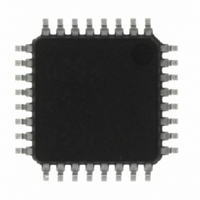
M37544G2AGP#U0 Renesas Electronics America, M37544G2AGP#U0 Datasheet - Page 64

M37544G2AGP#U0
Manufacturer Part Number
M37544G2AGP#U0
Description
IC 740 MCU OTP 8K 32LQFP
Manufacturer
Renesas Electronics America
Series
740/38000r
Specifications of M37544G2AGP#U0
Core Processor
740
Core Size
8-Bit
Speed
8MHz
Connectivity
SIO, UART/USART
Peripherals
WDT
Number Of I /o
25
Program Memory Size
8KB (8K x 8)
Program Memory Type
QzROM
Ram Size
256 x 8
Voltage - Supply (vcc/vdd)
4 V ~ 5.5 V
Data Converters
A/D 6x8b
Oscillator Type
Internal
Operating Temperature
-20°C ~ 85°C
Package / Case
32-LQFP
Lead Free Status / RoHS Status
Lead free / RoHS Compliant
Eeprom Size
-
Available stocks
Company
Part Number
Manufacturer
Quantity
Price
Rev.1.04
REJ03B0012-0104Z
7544 Group
Notes on Timers
1. When n (0 to 255) is written to a timer latch, the frequency divi-
2. When a count source of timer X is switched, stop a count of the
Notes on Timer 1
1. Timer 1 count source
The “on-chip oscillator output” of timer 1 count source selection
bits (bits 1 and 0 of timer count source set register 2 (address
2F
trol bit (bit 3 of CPU mode register (address 3B
oscillator oscillation enabled).
Notes on Timer A
1. CNTR
CNTR
switch bit (bit 6 of timer A mode register (address 1D
When this bit is “0”, the CNTR
the falling edge of the CNTR
the CNTR
the CNTR
However, in the pulse width HL continuously measurement mode,
CNTR
edges of CNTR
CNTR
2. Period measurement mode, event counter mode and pulse
width HL continuously measurement mode
Set the direction register of port P0
pin, to input.
Set the key-on wakeup function of P0
CNTR
lection bit (bit 7 of interrupt edge selection register (address 3A
to “1”.
3. Timer A count source
The “on-chip oscillator output” of timer A count source selection
bits (bits 3 and 2 of timer count source set register 2 (address
2F
trol bit (bit 3 of CPU mode register (address 3B
oscillator oscillation enabled).
sion ratio is 1/(n+1).
timer.
16
16
)) can be selected while the on-chip oscillator oscillation con-
)) can be selected while the on-chip oscillator oscillation con-
1
1
1
1
active edge switch bit.
interrupt active edge depends on the CNTR
pin, to be disabled by setting the P0
interrupt request is generated at both rising and falling
1
1
1
interrupt active edge selection
pin input signal.
interrupt request bit goes to “1” at the rising edge of
2004.06.08
1
pin input signal regardless of the setting of
page 62 of 66
1
pin input signal. When this bit is “1”,
1
interrupt request bit goes to “1” at
0
, which is also used as CNTR
0
, which is also used as
0
key-on wakeup se-
16
16
)) is “0” (on-chip
)) is “0” (on-chip
1
16
active edge
)).
16
))
1
Notes on Timer X
1. CNTR
CNTR
switch bit (bit 2 of timer X mode register (address 2B
When this bit is “0”, the CNTR
the falling edge of CNTR
CNTR
CNTR
2. Timer X count source selection
The f(X
count source selection bits (bits 1 and 0 of timer count source set
register 1 (address 2E
on-chip oscillator is selected.
Do not select it for the timer X count source at the RC oscillation.
3. Pulse output mode
Set the direction register of port P1
pin, to output.
When the TX
which is also used as TX
4. Pulse width measurement mode
Set the direction register of port P1
pin, to input.
0
0
0
IN
pin input signal.
interrupt active edge depends on the CNTR
interrupt request bit goes to “1” at the rising edge of
0
) (frequency not divided) can be selected by the timer X
interrupt active edge selection
OUT
pin is used, set the direction register of port P0
16
)) only when the ceramic oscillation or the
0
OUT
pin input signal. When this bit is “1”, the
pin, to output.
0
interrupt request bit goes to “1” at
4
4
, which is also used as CNTR
, which is also used as CNTR
0
16
active edge
)).
3
0
0
,


