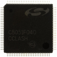
C8051F040-GQ Silicon Laboratories Inc, C8051F040-GQ Datasheet - Page 210

C8051F040-GQ
Manufacturer Part Number
C8051F040-GQ
Description
IC 8051 MCU 64K FLASH 100TQFP
Manufacturer
Silicon Laboratories Inc
Series
C8051F04xr
Datasheets
1.C8051F040-TB.pdf
(328 pages)
2.C8051F040-TB.pdf
(2 pages)
3.C8051F043-GQ.pdf
(328 pages)
Specifications of C8051F040-GQ
Program Memory Type
FLASH
Program Memory Size
64KB (64K x 8)
Package / Case
100-TQFP, 100-VQFP
Core Processor
8051
Core Size
8-Bit
Speed
25MHz
Connectivity
CAN, EBI/EMI, SMBus (2-Wire/I²C), SPI, UART/USART
Peripherals
Brown-out Detect/Reset, POR, PWM, Temp Sensor, WDT
Number Of I /o
64
Ram Size
4.25K x 8
Voltage - Supply (vcc/vdd)
2.7 V ~ 3.6 V
Data Converters
A/D 8x8b, 13x12b; D/A 2x10b, 2x12b
Oscillator Type
Internal
Operating Temperature
-40°C ~ 85°C
Processor Series
C8051F0x
Core
8051
Data Bus Width
8 bit
Data Ram Size
4.25 KB
Interface Type
CAN/SMBus/SPI/UART
Maximum Clock Frequency
25 MHz
Number Of Programmable I/os
64
Number Of Timers
5
Operating Supply Voltage
2.7 V to 3.6 V
Maximum Operating Temperature
+ 85 C
Mounting Style
SMD/SMT
3rd Party Development Tools
PK51, CA51, A51, ULINK2
Development Tools By Supplier
C8051F040DK
Minimum Operating Temperature
- 40 C
On-chip Adc
8-ch x 8-bit or 13-ch x 12-bit
On-chip Dac
2-ch x 12-bit
No. Of I/o's
64
Ram Memory Size
4352Byte
Cpu Speed
25MHz
No. Of Timers
5
Rohs Compliant
Yes
Data Rom Size
64 KB
A/d Bit Size
12 bit
A/d Channels Available
13
Height
1 mm
Length
14 mm
Supply Voltage (max)
3.6 V
Supply Voltage (min)
2.7 V
Width
14 mm
Package
100TQFP
Device Core
8051
Family Name
C8051F04x
Maximum Speed
25 MHz
Lead Free Status / RoHS Status
Lead free / RoHS Compliant
For Use With
336-1205 - DEV KIT FOR F040/F041/F042/F043
Eeprom Size
-
Lead Free Status / Rohs Status
Lead free / RoHS Compliant
Other names
336-1204
Available stocks
Company
Part Number
Manufacturer
Quantity
Price
Company:
Part Number:
C8051F040-GQ
Manufacturer:
SiliconL
Quantity:
702
Company:
Part Number:
C8051F040-GQ
Manufacturer:
Silicon Laboratories Inc
Quantity:
10 000
Company:
Part Number:
C8051F040-GQR
Manufacturer:
Silicon Laboratories Inc
Quantity:
10 000
Part Number:
C8051F040-GQR
Manufacturer:
SILICON LABS/芯科
Quantity:
20 000
C8051F040/1/2/3/4/5/6/7
17.1.6. External Memory Interface Pin Assignments
If the External Memory Interface (EMIF) is enabled on the Low ports (Ports 0 through 3), EMIFLE (XBR2.5)
should be set to a logic 1 so that the Crossbar will not assign peripherals to P0.7 (/WR), P0.6 (/RD), and, if
the External Memory Interface is in Multiplexed mode, P0.5 (ALE). Figure 17.4 shows an example Cross-
bar Decode Table with EMIFLE=1 and the EMIF in Multiplexed mode. Figure 17.5 shows an example
Crossbar Decode Table with EMIFLE=1 and the EMIF in Non-multiplexed mode.
If the External Memory Interface is enabled on the Low ports and an off-chip MOVX operation occurs, the
External Memory Interface will control the output states (logic 1 or logic 0) of the affected Port pins during
the execution phase of the MOVX instruction, regardless of the settings of the Crossbar registers or the
Port Data registers. The output configuration (push-pull or open-drain) of the Port pins is not affected by
the EMIF operation, except that Read operations will explicitly disable the output drivers on the Data Bus.
In most cases, GPIO pins used in EMIF operations (especially the /WR and /RD lines) should be
configured as push-pull and ‘parked’ at a logic 1 state. See
Interface and On-Chip XRAM” on page 189
210
TX0
RX0
SCK
MISO
MOSI
NSS
SDA
SCL
TX1
RX1
CEX0
CEX1
CEX2
CEX3
CEX4
CEX5
ECI
CP0
CP1
CP2
T0
/INT0
T1
/INT1
T2
T2EX
T3
T3EX
T4
T4EX
/SYSCLK
CNVSTR0
CNVSTR2
PIN I/O 0
1
(EMIFLE = 1; EMIF in Multiplexed Mode; P1MDIN = 0xFF)
2
3
P0
4
5
Figure 17.4. Priority Crossbar Decode Table
6
7
0
AIN1 Inputs/Non-muxed Addr H Muxed Addr H/Non-muxed Addr L
1
2
NSS is not assigned to a port pin when the SPI is placed in 3-wire mode
3
P1
4
5
6
for more information about the External Memory Interface.
7
Rev. 1.4
0
1
2
3
P2
4
5
6
7
Section “16. External Data Memory
0
Muxed Data/Non-muxed Data
1
2
3
P3
4
5
6
7
Crossbar Register Bits
UART0EN:
UART1EN:
CNVSTE0: XBR2.0
CNVSTE2: XBR3.2
SMB0EN:
PCA0ME:
SYSCKE: XBR1.7
SPI0EN:
T2EXE: XBR1.6
T3EXE: XBR3.1
T4EXE: XBR2.4
ECI0E: XBR0.6
INT0E: XBR1.2
INT1E: XBR1.4
CP0E: XBR0.7
CP1E: XBR1.0
CP2E: XBR3.3
T0E: XBR1.1
T1E: XBR1.3
T2E: XBR1.5
T3E: XBR3.0
T4E: XBR2.3
XBR0.2
XBR0.1
XBR0.0
XBR2.2
XBR0.[5:3]


