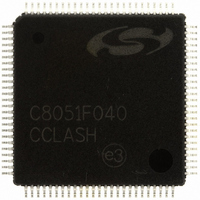
C8051F040-GQ Silicon Laboratories Inc, C8051F040-GQ Datasheet - Page 74

C8051F040-GQ
Manufacturer Part Number
C8051F040-GQ
Description
IC 8051 MCU 64K FLASH 100TQFP
Manufacturer
Silicon Laboratories Inc
Series
C8051F04xr
Datasheets
1.C8051F040-TB.pdf
(328 pages)
2.C8051F040-TB.pdf
(2 pages)
3.C8051F043-GQ.pdf
(328 pages)
Specifications of C8051F040-GQ
Program Memory Type
FLASH
Program Memory Size
64KB (64K x 8)
Package / Case
100-TQFP, 100-VQFP
Core Processor
8051
Core Size
8-Bit
Speed
25MHz
Connectivity
CAN, EBI/EMI, SMBus (2-Wire/I²C), SPI, UART/USART
Peripherals
Brown-out Detect/Reset, POR, PWM, Temp Sensor, WDT
Number Of I /o
64
Ram Size
4.25K x 8
Voltage - Supply (vcc/vdd)
2.7 V ~ 3.6 V
Data Converters
A/D 8x8b, 13x12b; D/A 2x10b, 2x12b
Oscillator Type
Internal
Operating Temperature
-40°C ~ 85°C
Processor Series
C8051F0x
Core
8051
Data Bus Width
8 bit
Data Ram Size
4.25 KB
Interface Type
CAN/SMBus/SPI/UART
Maximum Clock Frequency
25 MHz
Number Of Programmable I/os
64
Number Of Timers
5
Operating Supply Voltage
2.7 V to 3.6 V
Maximum Operating Temperature
+ 85 C
Mounting Style
SMD/SMT
3rd Party Development Tools
PK51, CA51, A51, ULINK2
Development Tools By Supplier
C8051F040DK
Minimum Operating Temperature
- 40 C
On-chip Adc
8-ch x 8-bit or 13-ch x 12-bit
On-chip Dac
2-ch x 12-bit
No. Of I/o's
64
Ram Memory Size
4352Byte
Cpu Speed
25MHz
No. Of Timers
5
Rohs Compliant
Yes
Data Rom Size
64 KB
A/d Bit Size
12 bit
A/d Channels Available
13
Height
1 mm
Length
14 mm
Supply Voltage (max)
3.6 V
Supply Voltage (min)
2.7 V
Width
14 mm
Package
100TQFP
Device Core
8051
Family Name
C8051F04x
Maximum Speed
25 MHz
Lead Free Status / RoHS Status
Lead free / RoHS Compliant
For Use With
336-1205 - DEV KIT FOR F040/F041/F042/F043
Eeprom Size
-
Lead Free Status / Rohs Status
Lead free / RoHS Compliant
Other names
336-1204
Available stocks
Company
Part Number
Manufacturer
Quantity
Price
Company:
Part Number:
C8051F040-GQ
Manufacturer:
SiliconL
Quantity:
702
Company:
Part Number:
C8051F040-GQ
Manufacturer:
Silicon Laboratories Inc
Quantity:
10 000
Company:
Part Number:
C8051F040-GQR
Manufacturer:
Silicon Laboratories Inc
Quantity:
10 000
Part Number:
C8051F040-GQR
Manufacturer:
SILICON LABS/芯科
Quantity:
20 000
C8051F040/1/2/3/4/5/6/7
6.2.
The High Voltage Difference Amplifier (HVDA) can be used to measure high differential voltages up to 60 V
peak-to-peak, reject high common-mode voltages up to ±60 V, and condition the signal voltage range to be
suitable for input to ADC0. The input signal to the HVDA may be below AGND to -60 volts, and as high as
+60 volts, making the device suitable for both single and dual supply applications. The HVDA will provides
a common-mode signal for the ADC via the High Voltage Reference Input (HVREF), allowing measure-
ment of signals outside the specified ADC input range using on-chip circuitry. The HVDA has a gain of
0.05 V/V to 14 V/V. The first stage 20:1 difference amplifier has a gain of 0.05 V/V when the output ampli-
fier is used as a unity gain buffer. When the output amplifier is set to a gain of 280 (selected using the
HVGAIN bits in the High Voltage Control Register), the overall gain of 14 can be attained. The HVDA is
factory calibrated for a high common-mode rejection of 72 dB.
The HVDA uses four available external pins: +HVAIN, -HVAIN, HVCAP, and the aforementioned HVREF.
HVAIN+ and HVAIN- serve as the differential inputs to the HVDA. HVREF can be used to provide a com-
mon mode reference for input to ADC0. HVCAP facilitates the use of a capacitor for noise filtering in con-
junction with R7 (see Figure 6.3 for R7 and other approximate resistor values). Alternatively, the HVCAP
could also be used to access amplification of the first stage of the HVDA at an external pin. (See Table 6.3
on page 90 for electrical specifications of the HVDA.)
Note: The output voltage of the HVDA is selected as an input to ADC0 via its analog multiplexer (AMUX0). HVDA
74
HVAIN+
HVAIN-
output voltages greater than the ADC0 reference voltage (Vref) or less than 0 volts (with respect to analog
ground) will result in saturation (output codes > full-scale or output codes < 0 respectively.) Allow for adequate
settle/tracking time for proper voltage measurements.
High Voltage Difference Amplifier
Figure 6.3. High Voltage Difference Amplifier Functional Diagram
Resistor values are
Equation 6.1. Calculating HVDA Output Voltage to ADC0
approximate
V
100 k Ω
100k Ω
OUT
=
5k Ω
5k Ω
[
(
HVAIN+
HVREF
)
–
Rev. 1.4
(
HVAIN-
HVA0CN
)
] Gain
5k Ω
⋅
HVCAP
+
Gain Setting
HVREF
(To AMUX0)
Vout


