C8051F061-GQ Silicon Laboratories Inc, C8051F061-GQ Datasheet - Page 318
C8051F061-GQ
Manufacturer Part Number
C8051F061-GQ
Description
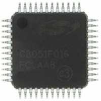
IC 8051 MCU 64K FLASH 64TQFP
Manufacturer
Silicon Laboratories Inc
Series
C8051F06xr
Specifications of C8051F061-GQ
Program Memory Type
FLASH
Program Memory Size
64KB (64K x 8)
Package / Case
64-TQFP, 64-VQFP
Core Processor
8051
Core Size
8-Bit
Speed
25MHz
Connectivity
CAN, SMBus (2-Wire/I²C), SPI, UART/USART
Peripherals
Brown-out Detect/Reset, POR, PWM, Temp Sensor, WDT
Number Of I /o
24
Ram Size
4.25K x 8
Voltage - Supply (vcc/vdd)
2.7 V ~ 3.6 V
Data Converters
A/D 2x16b, 8x10b; D/A 2x12b
Oscillator Type
Internal
Operating Temperature
-40°C ~ 85°C
Processor Series
C8051F0x
Core
8051
Data Bus Width
8 bit
Data Ram Size
4.25 KB
Interface Type
CAN/I2C/SMBus/SPI/UART
Maximum Clock Frequency
25 MHz
Number Of Programmable I/os
24
Number Of Timers
5
Operating Supply Voltage
2.7 V to 3.6 V
Maximum Operating Temperature
+ 85 C
Mounting Style
SMD/SMT
3rd Party Development Tools
PK51, CA51, A51, ULINK2
Development Tools By Supplier
C8051F060DK
Minimum Operating Temperature
- 40 C
On-chip Adc
2-ch x 16-bit
On-chip Dac
2-ch x 12-bit
Lead Free Status / RoHS Status
Lead free / RoHS Compliant
Eeprom Size
-
Lead Free Status / Rohs Status
Lead free / RoHS Compliant
Other names
336-1215
Available stocks
Company
Part Number
Manufacturer
Quantity
Price
Company:

Part Number:
C8051F061-GQ
Manufacturer:
Silicon Laboratories Inc
Quantity:
10 000
Company:
Part Number:
C8051F061-GQR
Manufacturer:
SILICON
Quantity:
2 100
Company:
Part Number:
C8051F061-GQR
Manufacturer:
Silicon Laboratories Inc
Quantity:
10 000


C8051F060/1/2/3/4/5/6/7
26.1. Boundary Scan
The DR in the Boundary Scan path is a 126-bit shift register for the
register for the C8051F061/3/5/7. The Boundary DR provides control and observability of all the device
pins as well as the SFR bus and Weak Pullup feature via the EXTEST and SAMPLE commands.
318
EXTEST provides access to both capture and update actions, while Sample only performs a capture.
24, 26, 28, 30, 32,
25, 27, 29, 31, 33,
40, 42, 44, 46, 48,
41, 43, 45, 47, 49,
56, 58, 60, 62, 64,
57, 59, 61, 63, 65,
78, 80, 82, 84, 86,
8, 10, 12, 14, 16,
9, 11, 13, 15, 17,
50, 52, 54
51, 53, 55
66, 68, 70
67, 69, 71
72, 74, 76
73, 75, 77
88, 90, 92
18, 20, 22
19, 21, 23
34, 36, 38
35, 37, 39
Bit
0
1
2
3
4
5
6
7
Table 26.1. Boundary Data Register Bit Definitions (C8051F060/2/4/6)
Action
Capture Reset Enable from MCU
Update
Capture Reset Input from /RST pin
Update
Capture CAN RX Output Enable to pin
Update
Capture CAN RX Input from pin
Update
Capture CAN TX Output Enable to pin
Update
Capture CAN TX Input from pin
Update
Capture External Clock from XTAL1 pin
Update
Capture Weak Pullup Enable from MCU
Update
Capture P0.n output enable from MCU (e.g. Bit 8 = P0.0, Bit 10 = P0.1, etc.)
Update
Capture P0.n input from pin (e.g. Bit 9 = P0.0, Bit 11 = P0.1, etc.)
Update
Capture P1.n output enable from MCU (follows P0.n numbering scheme)
Update
Capture P1.n input from pin (follows P0.n numbering scheme)
Update
Capture P2.n output enable from MCU (follows P0.n numbering scheme)
Update
Capture P2.n input from pin (follows P0.n numbering scheme)
Update
Capture P3.n output enable from MCU (follows P0.n numbering scheme)
Update
Capture P3.n input from pin (follows P0.n numbering scheme)
Update
Capture P4.5, P4.6, P4.7 (respectively) output enable from MCU
Update
Capture P4.5, P4.6, P4.7 (respectively) input from pin
Update
Capture P5.n output enable from MCU (follows P0.n numbering scheme)
Update
Target
Reset Enable to /RST pin
Not used
CAN RX Output Enable to pin
CAN RX Output to pin
CAN TX Output Enable to pin
CAN TX Output to pin
Not used
Weak Pullup Enable to Port Pins
P0.n output enable to pin (e.g. Bit 8 = P0.0oe, Bit 10 = P0.1oe, etc.)
P0.n output to pin (e.g. Bit 9 = P0.0, Bit 11 = P0.1, etc.)
P1.n output enable to pin (follows P0.n numbering scheme)
P1.n output to pin (follows P0.n numbering scheme)
P2.n output enable to pin (follows P0.n numbering scheme)
P2.n output to pin (follows P0.n numbering scheme)
P3.n output enable to pin (follows P0.n numbering scheme)
P3.n output to pin (follows P0.n numbering scheme)
P4.5, P4.6, P4.7 (respectively) output enable to pin
P4.5, P4.6, P4.7 (respectively) output to pin
P5.n output enable to pin (follows P0.n numbering scheme)
Rev. 1.2
C8051F060/2/4/6
and a 118-bit shift
Related parts for C8051F061-GQ
Image
Part Number
Description
Manufacturer
Datasheet
Request
R

Part Number:
Description:
SMD/C°/SINGLE-ENDED OUTPUT SILICON OSCILLATOR
Manufacturer:
Silicon Laboratories Inc
Part Number:
Description:
Manufacturer:
Silicon Laboratories Inc
Datasheet:
Part Number:
Description:
N/A N/A/SI4010 AES KEYFOB DEMO WITH LCD RX
Manufacturer:
Silicon Laboratories Inc
Datasheet:
Part Number:
Description:
N/A N/A/SI4010 SIMPLIFIED KEY FOB DEMO WITH LED RX
Manufacturer:
Silicon Laboratories Inc
Datasheet:
Part Number:
Description:
N/A/-40 TO 85 OC/EZLINK MODULE; F930/4432 HIGH BAND (REV E/B1)
Manufacturer:
Silicon Laboratories Inc
Part Number:
Description:
EZLink Module; F930/4432 Low Band (rev e/B1)
Manufacturer:
Silicon Laboratories Inc
Part Number:
Description:
I°/4460 10 DBM RADIO TEST CARD 434 MHZ
Manufacturer:
Silicon Laboratories Inc
Part Number:
Description:
I°/4461 14 DBM RADIO TEST CARD 868 MHZ
Manufacturer:
Silicon Laboratories Inc
Part Number:
Description:
I°/4463 20 DBM RFSWITCH RADIO TEST CARD 460 MHZ
Manufacturer:
Silicon Laboratories Inc
Part Number:
Description:
I°/4463 20 DBM RADIO TEST CARD 868 MHZ
Manufacturer:
Silicon Laboratories Inc
Part Number:
Description:
I°/4463 27 DBM RADIO TEST CARD 868 MHZ
Manufacturer:
Silicon Laboratories Inc
Part Number:
Description:
I°/4463 SKYWORKS 30 DBM RADIO TEST CARD 915 MHZ
Manufacturer:
Silicon Laboratories Inc
Part Number:
Description:
N/A N/A/-40 TO 85 OC/4463 RFMD 30 DBM RADIO TEST CARD 915 MHZ
Manufacturer:
Silicon Laboratories Inc
Part Number:
Description:
I°/4463 20 DBM RADIO TEST CARD 169 MHZ
Manufacturer:
Silicon Laboratories Inc