MC9S12H128VFVE Freescale Semiconductor, MC9S12H128VFVE Datasheet - Page 62
MC9S12H128VFVE
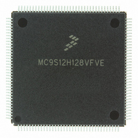
Manufacturer Part Number
MC9S12H128VFVE
Description
IC MCU 128K FLASH 16MHZ 144-LQFP
Manufacturer
Freescale Semiconductor
Series
HCS12r
Datasheet
1.MC9S12H256VFVER.pdf
(130 pages)
Specifications of MC9S12H128VFVE
Core Processor
HCS12
Core Size
16-Bit
Speed
16MHz
Connectivity
CAN, I²C, SCI, SPI
Peripherals
LCD, POR, PWM, WDT
Number Of I /o
99
Program Memory Size
128KB (128K x 8)
Program Memory Type
FLASH
Eeprom Size
4K x 8
Ram Size
6K x 8
Voltage - Supply (vcc/vdd)
2.35 V ~ 5.25 V
Data Converters
A/D 8x10b
Oscillator Type
Internal
Operating Temperature
-40°C ~ 105°C
Package / Case
144-LQFP
Processor Series
S12H
Core
HCS12
Data Bus Width
16 bit
Data Ram Size
6 KB
Interface Type
CAN/I2C/SCI/SPI
Maximum Clock Frequency
16 MHz
Number Of Programmable I/os
99
Number Of Timers
8
Operating Supply Voltage
- 0.3 V to + 6 V
Maximum Operating Temperature
+ 105 C
Mounting Style
SMD/SMT
3rd Party Development Tools
EWHCS12
Minimum Operating Temperature
- 40 C
On-chip Adc
16-ch x 10-bit
Package
144LQFP
Family Name
HCS12
Maximum Speed
16 MHz
Lead Free Status / RoHS Status
Lead free / RoHS Compliant
Available stocks
Company
Part Number
Manufacturer
Quantity
Price

Company:
Part Number:
MC9S12H128VFVE
Manufacturer:
Freescale Semiconductor
Quantity:
10 000


MC9S12H256 Device User Guide — V01.20
2.3.15 PE2 / FP20 / R/W — Port E I/O Pin 2
PE2 is a general purpose input or output pin. It can be configured as frontplane segment driver output FP20
of the LCD module. In MCU expanded modes of operations, this pin performs the read/write output signal
for the external bus. It indicates the direction of data on the external bus.
2.3.16 PE1 / IRQ — Port E Input Pin 1
PE1 is a general purpose input pin and also the maskable interrupt request input that provides a means of
applying asynchronous interrupt requests. This will wake up the MCU from STOP or WAIT mode.
2.3.17 PE0 / XIRQ — Port E Input Pin 0
PE0 is a general purpose input pin and also the non-maskable interrupt request input that provides a means
of applying asynchronous interrupt requests. This will wake up the MCU from STOP or WAIT mode.
2.3.18 PH[7:0] / KWH[7:0] — Port H I/O Pins [7:0]
PH7-PH0 are general purpose input or output pins. They can be configured to generate an interrupt causing
the MCU to exit STOP or WAIT mode.
2.3.19 PJ[3:0] / KWJ[3:0] — Port J I/O Pins [3:0]
PJ3-PJ0 are general purpose input or output pins. They can be configured to generate an interrupt causing
the MCU to exit STOP or WAIT mode.and are shared with the interrupt function.
2.3.20 PK7 / FP23 / ECS / ROMONE — Port K I/O Pin 7
PK7 is a general purpose input or output pin. It can be configured as frontplane segment driver output FP23
of the LCD module. During MCU expanded modes of operation, this pin is used as the emulation chip
select signal (ECS). During reset of the MCU to normal expanded modes of operation, this pin is used to
enable the Flash EEPROM memory in the memory map (ROMONE). At the rising edge of RESET, the
state of this pin is latched to the ROMON bit.
2.3.21 PK[3:0] / BP[3:0] / XADDR[17:14] — Port K I/O Pins [3:0]
PK3-PK0 are general purpose input or output pins. They can be configured as backplane segment driver
outputs BP3-BP0 of the LCD module. In MCU expanded modes of operation, these pins provide the
expanded address XADDR[17:14] for the external bus.
62
NOTE:
NOTE:
These pins are not available in the 112-pin LQFP version.
These pins are not available in the 112-pin LQFP version.
Related parts for MC9S12H128VFVE
Image
Part Number
Description
Manufacturer
Datasheet
Request
R

Part Number:
Description:
Manufacturer:
Freescale Semiconductor, Inc
Datasheet:
Part Number:
Description:
Manufacturer:
Freescale Semiconductor, Inc
Datasheet:
Part Number:
Description:
Manufacturer:
Freescale Semiconductor, Inc
Datasheet:
Part Number:
Description:
Manufacturer:
Freescale Semiconductor, Inc
Datasheet:
Part Number:
Description:
Manufacturer:
Freescale Semiconductor, Inc
Datasheet:
Part Number:
Description:
Manufacturer:
Freescale Semiconductor, Inc
Datasheet:
Part Number:
Description:
Manufacturer:
Freescale Semiconductor, Inc
Datasheet:
Part Number:
Description:
Manufacturer:
Freescale Semiconductor, Inc
Datasheet:
Part Number:
Description:
Manufacturer:
Freescale Semiconductor, Inc
Datasheet:
Part Number:
Description:
Manufacturer:
Freescale Semiconductor, Inc
Datasheet:
Part Number:
Description:
Manufacturer:
Freescale Semiconductor, Inc
Datasheet:
Part Number:
Description:
Manufacturer:
Freescale Semiconductor, Inc
Datasheet:
Part Number:
Description:
Manufacturer:
Freescale Semiconductor, Inc
Datasheet:
Part Number:
Description:
Manufacturer:
Freescale Semiconductor, Inc
Datasheet:
Part Number:
Description:
Manufacturer:
Freescale Semiconductor, Inc
Datasheet: