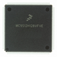
MC9S12H128VFVE Freescale Semiconductor, MC9S12H128VFVE Datasheet - Page 74

MC9S12H128VFVE
Manufacturer Part Number
MC9S12H128VFVE
Description
IC MCU 128K FLASH 16MHZ 144-LQFP
Manufacturer
Freescale Semiconductor
Series
HCS12r
Datasheet
1.MC9S12H256VFVER.pdf
(130 pages)
Specifications of MC9S12H128VFVE
Core Processor
HCS12
Core Size
16-Bit
Speed
16MHz
Connectivity
CAN, I²C, SCI, SPI
Peripherals
LCD, POR, PWM, WDT
Number Of I /o
99
Program Memory Size
128KB (128K x 8)
Program Memory Type
FLASH
Eeprom Size
4K x 8
Ram Size
6K x 8
Voltage - Supply (vcc/vdd)
2.35 V ~ 5.25 V
Data Converters
A/D 8x10b
Oscillator Type
Internal
Operating Temperature
-40°C ~ 105°C
Package / Case
144-LQFP
Processor Series
S12H
Core
HCS12
Data Bus Width
16 bit
Data Ram Size
6 KB
Interface Type
CAN/I2C/SCI/SPI
Maximum Clock Frequency
16 MHz
Number Of Programmable I/os
99
Number Of Timers
8
Operating Supply Voltage
- 0.3 V to + 6 V
Maximum Operating Temperature
+ 105 C
Mounting Style
SMD/SMT
3rd Party Development Tools
EWHCS12
Minimum Operating Temperature
- 40 C
On-chip Adc
16-ch x 10-bit
Package
144LQFP
Family Name
HCS12
Maximum Speed
16 MHz
Lead Free Status / RoHS Status
Lead free / RoHS Compliant
Available stocks
Company
Part Number
Manufacturer
Quantity
Price
Company:
Part Number:
MC9S12H128VFVE
Manufacturer:
Freescale Semiconductor
Quantity:
10 000
MC9S12H256 Device User Guide — V01.20
If an internal access is made while E, R/W, and LSTRB are configured as bus control outputs and internal
visibility is off (IVIS=0), E will remain low for the cycle, R/W will remain high, and address, data and the
LSTRB pins will remain at their previous state.
When internal visibility is enabled (IVIS=1), certain internal cycles will be blocked from going external.
During cycles when the BDM is selected, R/W will remain high, data will maintain its previous state, and
address and LSTRB pins will be updated with the internal value. During CPU no access cycles when the
BDM is not driving, R/W will remain high, and address, data and the LSTRB pins will remain at their
previous state.
4.2.1.5 Emulation Expanded Wide Mode
In expanded wide modes, Ports A and B are configured as a 16-bit multiplexed address and data bus and
Port E provides bus control and status signals. These signals allow external memory and peripheral devices
to be interfaced to the MCU. These signals can also be used by a logic analyzer to monitor the progress of
application programs.
The bus control related pins in Port E (PE7/NOACC, PE6/MODB/IPIPE1, PE5/MODA/IPIPE0,
PE4/ECLK, PE3/LSTRB/TAGLO, and PE2/R/W) are all configured to serve their bus control output
functions rather than general purpose I/O. Notice that writes to the bus control enable bits in the PEAR
register in special mode are restricted.
4.2.1.6 Emulation Expanded Narrow Mode
Expanded narrow modes are intended to allow connection of single 8-bit external memory devices for
lower cost systems that do not need the performance of a full 16-bit external data bus. Accesses to internal
resources that have been mapped external (i.e. PORTA, PORTB, DDRA, DDRB, PORTE, DDRE, PEAR,
PUCR, RDRIV) will be accessed with a 16-bit data bus on Ports A and B. Accesses of 16-bit external
words to addresses which are normally mapped external will be broken into two separate 8-bit accesses
using Port A as an 8-bit data bus. Internal operations continue to use full 16-bit data paths. They are only
visible externally as 16-bit information if IVIS=1.
Ports A and B are configured as multiplexed address and data output ports. During external accesses,
address A15, data D15 and D7 are associated with PA7, address A0 is associated with PB0 and data D8
and D0 are associated with PA0. During internal visible accesses and accesses to internal resources that
have been mapped external, address A15 and data D15 is associated with PA7 and address A0 and data
D0 is associated with PB0.
The bus control related pins in Port E (PE7/NOACC, PE6/MODB/IPIPE1, PE5/MODA/IPIPE0,
PE4/ECLK, PE3/LSTRB/TAGLO, and PE2/R/W) are all configured to serve their bus control output
functions rather than general purpose I/O. Notice that writes to the bus control enable bits in the PEAR
register in special mode are restricted.
4.2.2 Special Operating Modes
There are two special operating modes that correspond to normal operating modes. These operating modes
are commonly used in factory testing and system development.
74


