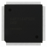
HD64F7144F50V Renesas Electronics America, HD64F7144F50V Datasheet - Page 95

HD64F7144F50V
Manufacturer Part Number
HD64F7144F50V
Description
IC SUPERH MCU FLASH 256K 112QFP
Manufacturer
Renesas Electronics America
Series
SuperH® SH7144r
Specifications of HD64F7144F50V
Core Processor
SH-2
Core Size
32-Bit
Speed
50MHz
Connectivity
EBI/EMI, I²C, SCI
Peripherals
DMA, POR, PWM, WDT
Number Of I /o
74
Program Memory Size
256KB (256K x 8)
Program Memory Type
FLASH
Ram Size
8K x 8
Voltage - Supply (vcc/vdd)
3 V ~ 3.6 V
Data Converters
A/D 8x10b
Oscillator Type
Internal
Operating Temperature
-20°C ~ 75°C
Package / Case
112-QFP
For Use With
HS0005KCU11H - EMULATOR E10A-USB H8S(X),SH2(A)EDK7145 - DEV EVALUATION KIT SH7145
Lead Free Status / RoHS Status
Lead free / RoHS Compliant
Eeprom Size
-
Available stocks
Company
Part Number
Manufacturer
Quantity
Price
Company:
Part Number:
HD64F7144F50V
Manufacturer:
RENESAS
Quantity:
450
Company:
Part Number:
HD64F7144F50V
Manufacturer:
Renesas Electronics America
Quantity:
10 000
Part Number:
HD64F7144F50V
Manufacturer:
RENESAS/瑞萨
Quantity:
20 000
- Current page: 95 of 531
- Download datasheet (3Mb)
The guard bit registers A0G and A1G can be specified for operands as independent registers.
Single data transfers use the IAB and IDB buses in place of the X bus and Y bus, so contention
occurs on the IDB bus between data transfers and instruction fetches.
Single data transfers handle word and longword data. Word data transfers involve only the top
word of the register. When data is loaded to a register, it goes to the top word and the bottom word
is automatically filled with zeros. If there are guard bits, the sign bit is extended to fill them. When
storing from a register, the top word is stored.
When a longword is transferred, 32 bits are valid. When loading a register that has guard bits, the
sign bit is extended to fill the guard bits.
When a guard bit register is stored, the top 24 bits become undefined, and the read out is to the
IDB bus. When the guard bit registers A0G and A1G load word data as the destination registers of
the MOVS.W instruction, the bottom byte is written to the register.
Figure 4.20 Single Data Transfer Flowchart (Word)
X0
X1
A0
A1
: Not affected for storing; cleared for loading. See
: Cannot be set
Pointer (R2, R3, R4, R5)
the text for information about A0G and A1G.
All memory areas
IAB[31:0]
IDB[15:0]
Y0
Y1
M0
M1
A0G
–2, 0, +2, +R8
Rev. 5.00 Jun 30, 2004 page 79 of 512
A1G DSR
Section 4 Instruction Features
REJ09B0171-0500O
Related parts for HD64F7144F50V
Image
Part Number
Description
Manufacturer
Datasheet
Request
R

Part Number:
Description:
KIT STARTER FOR M16C/29
Manufacturer:
Renesas Electronics America
Datasheet:

Part Number:
Description:
KIT STARTER FOR R8C/2D
Manufacturer:
Renesas Electronics America
Datasheet:

Part Number:
Description:
R0K33062P STARTER KIT
Manufacturer:
Renesas Electronics America
Datasheet:

Part Number:
Description:
KIT STARTER FOR R8C/23 E8A
Manufacturer:
Renesas Electronics America
Datasheet:

Part Number:
Description:
KIT STARTER FOR R8C/25
Manufacturer:
Renesas Electronics America
Datasheet:

Part Number:
Description:
KIT STARTER H8S2456 SHARPE DSPLY
Manufacturer:
Renesas Electronics America
Datasheet:

Part Number:
Description:
KIT STARTER FOR R8C38C
Manufacturer:
Renesas Electronics America
Datasheet:

Part Number:
Description:
KIT STARTER FOR R8C35C
Manufacturer:
Renesas Electronics America
Datasheet:

Part Number:
Description:
KIT STARTER FOR R8CL3AC+LCD APPS
Manufacturer:
Renesas Electronics America
Datasheet:

Part Number:
Description:
KIT STARTER FOR RX610
Manufacturer:
Renesas Electronics America
Datasheet:

Part Number:
Description:
KIT STARTER FOR R32C/118
Manufacturer:
Renesas Electronics America
Datasheet:

Part Number:
Description:
KIT DEV RSK-R8C/26-29
Manufacturer:
Renesas Electronics America
Datasheet:

Part Number:
Description:
KIT STARTER FOR SH7124
Manufacturer:
Renesas Electronics America
Datasheet:

Part Number:
Description:
KIT STARTER FOR H8SX/1622
Manufacturer:
Renesas Electronics America
Datasheet:


