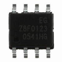
Z8F0123SB005EG Zilog, Z8F0123SB005EG Datasheet - Page 148

Z8F0123SB005EG
Manufacturer Part Number
Z8F0123SB005EG
Description
IC ENCORE MCU FLASH 1K 8SOIC
Manufacturer
Zilog
Series
Encore!® XP®r
Datasheet
1.Z8F0223SB005SG.pdf
(247 pages)
Specifications of Z8F0123SB005EG
Core Processor
Z8
Core Size
8-Bit
Speed
5MHz
Connectivity
IrDA, UART/USART
Peripherals
Brown-out Detect/Reset, LED, POR, PWM, WDT
Number Of I /o
6
Program Memory Size
1KB (1K x 8)
Program Memory Type
FLASH
Ram Size
256 x 8
Voltage - Supply (vcc/vdd)
2.7 V ~ 3.6 V
Data Converters
A/D 4x10b
Oscillator Type
Internal
Operating Temperature
-40°C ~ 105°C
Package / Case
8-SOIC (3.9mm Width)
Lead Free Status / RoHS Status
Lead free / RoHS Compliant
Eeprom Size
-
Other names
269-3757
- Current page: 148 of 247
- Download datasheet (4Mb)
Table 81. Flash Page Select Register (FPS)
BITS
FIELD
RESET
R/W
ADDR
PS024314-0308
Flash Page Select Register
INFO_EN
R/W
7
0
Reserved—0 when read
FSTAT—Flash Controller Status
000000 = Flash Controller locked
000001 = First unlock command received (73H written)
000010 = Second unlock command received (8CH written)
000011 = Flash Controller unlocked
000100 = Sector protect register selected
001xxx = Program operation in progress
010xxx = Page erase operation in progress
100xxx = Mass erase operation in progress
The Flash Page Select (FPS) register shares address space with the Flash Sector Protect
Register. Unless the Flash controller is unlocked and written with
address target the Flash Page Select Register.
The register is used to select one of the eight available Flash memory pages to be pro-
grammed or erased. Each Flash Page contains 512 bytes of Flash memory. During a Page
Erase operation, all Flash memory having addresses with the most significant 7-bits given
by FPS[6:0] are chosen for program/erase operation.
INFO_EN—Information Area Enable
0 = Information Area us not selected
1 = Information Area is selected. The Information Area is mapped into the Program Mem-
ory address space at addresses FE00H through FFFFH.
PAGE—Page Select
This 7-bit field identifies the Flash memory page for Page Erase and page unlocking.
Program Memory Address[15:9] = PAGE[6:0]. For the Z8F04x3 devices, the upper 4 bits
must always be 0. For the Z8F02x3 devices, the upper 5 bits must always be 0. For the
Z8F01x3 devices, the upper 6 bits must always be 0.
R/W
6
0
R/W
5
0
R/W
4
0
FF9H
PAGE
R/W
3
0
Z8 Encore! XP
R/W
2
0
Product Specification
5EH
, writes to this
R/W
1
0
®
F0823 Series
Flash Memory
R/W
0
0
138
Related parts for Z8F0123SB005EG
Image
Part Number
Description
Manufacturer
Datasheet
Request
R

Part Number:
Description:
Communication Controllers, ZILOG INTELLIGENT PERIPHERAL CONTROLLER (ZIP)
Manufacturer:
Zilog, Inc.
Datasheet:

Part Number:
Description:
KIT DEV FOR Z8 ENCORE 16K TO 64K
Manufacturer:
Zilog
Datasheet:

Part Number:
Description:
KIT DEV Z8 ENCORE XP 28-PIN
Manufacturer:
Zilog
Datasheet:

Part Number:
Description:
DEV KIT FOR Z8 ENCORE 8K/4K
Manufacturer:
Zilog
Datasheet:

Part Number:
Description:
KIT DEV Z8 ENCORE XP 28-PIN
Manufacturer:
Zilog
Datasheet:

Part Number:
Description:
DEV KIT FOR Z8 ENCORE 4K TO 8K
Manufacturer:
Zilog
Datasheet:

Part Number:
Description:
CMOS Z8 microcontroller. ROM 16 Kbytes, RAM 256 bytes, speed 16 MHz, 32 lines I/O, 3.0V to 5.5V
Manufacturer:
Zilog, Inc.
Datasheet:

Part Number:
Description:
Low-cost microcontroller. 512 bytes ROM, 61 bytes RAM, 8 MHz
Manufacturer:
Zilog, Inc.
Datasheet:

Part Number:
Description:
Z8 4K OTP Microcontroller
Manufacturer:
Zilog, Inc.
Datasheet:

Part Number:
Description:
CMOS SUPER8 ROMLESS MCU
Manufacturer:
Zilog, Inc.
Datasheet:

Part Number:
Description:
SL1866 CMOSZ8 OTP Microcontroller
Manufacturer:
Zilog, Inc.
Datasheet:

Part Number:
Description:
SL1866 CMOSZ8 OTP Microcontroller
Manufacturer:
Zilog, Inc.
Datasheet:

Part Number:
Description:
OTP (KB) = 1, RAM = 125, Speed = 12, I/O = 14, 8-bit Timers = 2, Comm Interfaces Other Features = Por, LV Protect, Voltage = 4.5-5.5V
Manufacturer:
Zilog, Inc.
Datasheet:

Part Number:
Description:
Manufacturer:
Zilog, Inc.
Datasheet:


