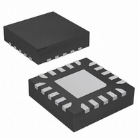
ATTINY24A-MMH Atmel, ATTINY24A-MMH Datasheet - Page 132

ATTINY24A-MMH
Manufacturer Part Number
ATTINY24A-MMH
Description
MCU AVR 2K FLASH 20MHZ 20VQFN
Manufacturer
Atmel
Series
AVR® ATtinyr
Specifications of ATTINY24A-MMH
Core Processor
AVR
Core Size
8-Bit
Speed
20MHz
Connectivity
USI
Peripherals
Brown-out Detect/Reset, POR, PWM, Temp Sensor, WDT
Number Of I /o
12
Program Memory Size
2KB (1K x 16)
Program Memory Type
FLASH
Eeprom Size
128 x 8
Ram Size
128 x 8
Voltage - Supply (vcc/vdd)
1.8 V ~ 5.5 V
Data Converters
A/D 8x10b
Oscillator Type
Internal
Operating Temperature
-40°C ~ 85°C
Package / Case
20-MLF®, QFN
Processor Series
ATTINY2x
Core
AVR8
Data Bus Width
8 bit
Data Ram Size
128 B
Interface Type
SPI, USI
Maximum Clock Frequency
20 MHz
Number Of Programmable I/os
12
Number Of Timers
2
Maximum Operating Temperature
+ 85 C
Mounting Style
SMD/SMT
3rd Party Development Tools
EWAVR, EWAVR-BL
Development Tools By Supplier
ATAVRDRAGON, ATSTK500, ATSTK600, ATAVRISP2, ATAVRONEKIT
Minimum Operating Temperature
- 40 C
On-chip Adc
10 bit, 20 Channel
For Use With
ATSTK505 - ADAPTER KIT FOR 14PIN AVR MCU
Lead Free Status / RoHS Status
Lead free / RoHS Compliant
- Current page: 132 of 286
- Download datasheet (10Mb)
16. Analog to Digital Converter
16.1
16.2
132
Features
Overview
ATtiny24A/44A/84A
•
•
•
•
•
•
•
•
•
•
•
•
•
•
•
•
•
ATtiny24A/44A/84A features a 10-bit, successive approximation Analog-to-Digital Converter
(ADC). The ADC is wired to a nine-channel analog multiplexer, which allows the ADC to mea-
sure the voltage at eight single-ended input pins, or between twelve differential pairs of input
pins, or from one internal, single-ended voltage channel coming from the internal temperature
sensor. Single-ended voltage inputs are referred to 0V (GND), while differential-ended input
pairs are subject to a gain stage with programmable amplification steps of 0 dB (1x) and 26 dB
(20x).
The ADC contains a Sample and Hold circuit which ensures that the input voltage to the ADC is
held at a constant level during conversion. A block diagram of the ADC is shown in
on page
Internal reference voltage of nominally 1.1V is provided on-chip. Alternatively, V
as reference voltage for single ended channels. There is also an option to use an external volt-
age reference and turn-off the internal voltage reference.
10-bit Resolution
1 LSB Integral Non-linearity
±2 LSB Absolute Accuracy
13 µs Conversion Time
15 kSPS at Maximum Resolution
Eight Multiplexed Single Ended Input Channels
Twelve Differential Input Channels with Selectable Gain (1x, 20x)
Temperature Sensor Input Channel
Optional Left Adjustment for ADC Result Readout
0 - V
1.1V ADC Reference Voltage
Free Running or Single Conversion Mode
ADC Start Conversion by Auto Triggering on Interrupt Sources
Interrupt on ADC Conversion Complete
Sleep Mode Noise Canceler
Unipolar / Bipolar Input Mode
Input Polarity Reversal Mode
CC
133.
ADC Input Voltage Range
CC
8183C–AVR–03/11
can be used
Figure 16-1
Related parts for ATTINY24A-MMH
Image
Part Number
Description
Manufacturer
Datasheet
Request
R

Part Number:
Description:
Manufacturer:
Atmel Corporation
Datasheet:

Part Number:
Description:
Manufacturer:
Atmel Corporation
Datasheet:

Part Number:
Description:
IC MCU AVR 2K FLASH 20MHZ 20-QFN
Manufacturer:
Atmel
Datasheet:

Part Number:
Description:
IC MCU AVR 2K FLASH 20MHZ 14SOIC
Manufacturer:
Atmel
Datasheet:

Part Number:
Description:
MCU AVR 2K FLASH 15MHZ 20-QFN
Manufacturer:
Atmel
Datasheet:

Part Number:
Description:
IC MCU AVR 2K FLASH 20MHZ 14-DIP
Manufacturer:
Atmel
Datasheet:

Part Number:
Description:
MCU AVR 2KB FLASH 20MHZ 14SOIC
Manufacturer:
Atmel
Datasheet:

Part Number:
Description:
MCU AVR 2KB FLASH 20MHZ 20QFN
Manufacturer:
Atmel
Datasheet:

Part Number:
Description:
MCU AVR 2K FLASH 15MHZ 14-SOIC
Manufacturer:
Atmel
Datasheet:

Part Number:
Description:
DEV KIT FOR AVR/AVR32
Manufacturer:
Atmel
Datasheet:

Part Number:
Description:
INTERVAL AND WIPE/WASH WIPER CONTROL IC WITH DELAY
Manufacturer:
ATMEL Corporation
Datasheet:

Part Number:
Description:
Low-Voltage Voice-Switched IC for Hands-Free Operation
Manufacturer:
ATMEL Corporation
Datasheet:


