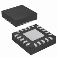
ATTINY24A-MMH Atmel, ATTINY24A-MMH Datasheet - Page 85

ATTINY24A-MMH
Manufacturer Part Number
ATTINY24A-MMH
Description
MCU AVR 2K FLASH 20MHZ 20VQFN
Manufacturer
Atmel
Series
AVR® ATtinyr
Specifications of ATTINY24A-MMH
Core Processor
AVR
Core Size
8-Bit
Speed
20MHz
Connectivity
USI
Peripherals
Brown-out Detect/Reset, POR, PWM, Temp Sensor, WDT
Number Of I /o
12
Program Memory Size
2KB (1K x 16)
Program Memory Type
FLASH
Eeprom Size
128 x 8
Ram Size
128 x 8
Voltage - Supply (vcc/vdd)
1.8 V ~ 5.5 V
Data Converters
A/D 8x10b
Oscillator Type
Internal
Operating Temperature
-40°C ~ 85°C
Package / Case
20-MLF®, QFN
Processor Series
ATTINY2x
Core
AVR8
Data Bus Width
8 bit
Data Ram Size
128 B
Interface Type
SPI, USI
Maximum Clock Frequency
20 MHz
Number Of Programmable I/os
12
Number Of Timers
2
Maximum Operating Temperature
+ 85 C
Mounting Style
SMD/SMT
3rd Party Development Tools
EWAVR, EWAVR-BL
Development Tools By Supplier
ATAVRDRAGON, ATSTK500, ATSTK600, ATAVRISP2, ATAVRONEKIT
Minimum Operating Temperature
- 40 C
On-chip Adc
10 bit, 20 Channel
For Use With
ATSTK505 - ADAPTER KIT FOR 14PIN AVR MCU
Lead Free Status / RoHS Status
Lead free / RoHS Compliant
- Current page: 85 of 286
- Download datasheet (10Mb)
12. 16-bit Timer/Counter1
12.1
12.2
8183C–AVR–03/11
Features
Overview
•
•
•
•
•
•
•
•
•
•
•
The 16-bit Timer/Counter unit allows accurate program execution timing (event management),
wave generation, and signal timing measurement.
A simplified block diagram of the 16-bit Timer/Counter is shown in
actual placement of I/O pins, refer to
I/O Registers, including I/O bits and I/O pins, are shown in bold. The device-specific I/O Register
and bit locations are listed in the
Figure 12-1.
True 16-bit Design (i.e., Allows 16-bit PWM)
Two independent Output Compare Units
Double Buffered Output Compare Registers
One Input Capture Unit
Input Capture Noise Canceler
Clear Timer on Compare Match (Auto Reload)
Glitch-free, Phase Correct Pulse Width Modulator (PWM)
Variable PWM Period
Frequency Generator
External Event Counter
Four independent interrupt Sources (TOV1, OCF1A, OCF1B, and ICF1)
16-bit Timer/Counter Block Diagram
Timer/Counter
TCCRnA
OCRnA
OCRnB
TCNTn
ICRn
=
=
“Register Description” on page
Direction
Count
Clear
“Pinout of ATtiny24A/44A/84A” on page
Control Logic
TOP
=
TCCRnB
Values
BOTTOM
Fixed
TOP
ICFn (Int.Req.)
clk
Detector
Edge
=
Tn
0
ATtiny24A/44A/84A
OCnA
(Int.Req.)
OCnB
(Int.Req.)
TOVn
(Int.Req.)
Clock Select
106.
Generation
Generation
( From Prescaler )
Waveform
Waveform
Canceler
Detector
Noise
Edge
Figure 12-1 on page
Comparator Ouput )
( From Analog
2. CPU accessible
OCnA
OCnB
ICPn
Tn
85. For
85
Related parts for ATTINY24A-MMH
Image
Part Number
Description
Manufacturer
Datasheet
Request
R

Part Number:
Description:
Manufacturer:
Atmel Corporation
Datasheet:

Part Number:
Description:
Manufacturer:
Atmel Corporation
Datasheet:

Part Number:
Description:
IC MCU AVR 2K FLASH 20MHZ 20-QFN
Manufacturer:
Atmel
Datasheet:

Part Number:
Description:
IC MCU AVR 2K FLASH 20MHZ 14SOIC
Manufacturer:
Atmel
Datasheet:

Part Number:
Description:
MCU AVR 2K FLASH 15MHZ 20-QFN
Manufacturer:
Atmel
Datasheet:

Part Number:
Description:
IC MCU AVR 2K FLASH 20MHZ 14-DIP
Manufacturer:
Atmel
Datasheet:

Part Number:
Description:
MCU AVR 2KB FLASH 20MHZ 14SOIC
Manufacturer:
Atmel
Datasheet:

Part Number:
Description:
MCU AVR 2KB FLASH 20MHZ 20QFN
Manufacturer:
Atmel
Datasheet:

Part Number:
Description:
MCU AVR 2K FLASH 15MHZ 14-SOIC
Manufacturer:
Atmel
Datasheet:

Part Number:
Description:
DEV KIT FOR AVR/AVR32
Manufacturer:
Atmel
Datasheet:

Part Number:
Description:
INTERVAL AND WIPE/WASH WIPER CONTROL IC WITH DELAY
Manufacturer:
ATMEL Corporation
Datasheet:

Part Number:
Description:
Low-Voltage Voice-Switched IC for Hands-Free Operation
Manufacturer:
ATMEL Corporation
Datasheet:


