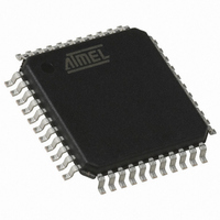
AT80C51RD2-RLRUM Atmel, AT80C51RD2-RLRUM Datasheet - Page 22

AT80C51RD2-RLRUM
Manufacturer Part Number
AT80C51RD2-RLRUM
Description
IC MCU 80C51 HI PERFORM 44VQFP
Manufacturer
Atmel
Series
80Cr
Datasheet
1.AT80C51RD2-RLRUM.pdf
(81 pages)
Specifications of AT80C51RD2-RLRUM
Core Processor
8051
Core Size
8-Bit
Speed
40MHz
Connectivity
UART/USART
Peripherals
POR, PWM, WDT
Number Of I /o
32
Program Memory Type
ROMless
Ram Size
1K x 8
Voltage - Supply (vcc/vdd)
2.7 V ~ 5.5 V
Oscillator Type
Internal
Operating Temperature
-40°C ~ 85°C
Package / Case
44-TQFP, 44-VQFP
Processor Series
AT80x
Core
8051
Data Bus Width
8 bit
Data Ram Size
1280 B
Interface Type
UART, SPI
Maximum Clock Frequency
60 MHz
Number Of Programmable I/os
32
Number Of Timers
3
Operating Supply Voltage
2.7 V to 5.5 V
Maximum Operating Temperature
+ 85 C
Mounting Style
SMD/SMT
3rd Party Development Tools
PK51, CA51, A51, ULINK2
Minimum Operating Temperature
- 40 C
Lead Free Status / RoHS Status
Lead free / RoHS Compliant
Eeprom Size
-
Program Memory Size
-
Data Converters
-
Lead Free Status / Rohs Status
Details
Available stocks
Company
Part Number
Manufacturer
Quantity
Price
Company:
Part Number:
AT80C51RD2-RLRUM
Manufacturer:
NXP
Quantity:
8 243
10. Programmable Counter Array (PCA)
22
AT80C51RD2
The PCA provides more timing capabilities with less CPU intervention than the standard
timer/counters. Its advantages include reduced software overhead and improved accuracy. The
PCA consists of a dedicated timer/counter which serves as the time base for an array of five
compare/capture modules. Its clock input can be programmed to count any one of the following
signals:
Each compare/capture modules can be programmed in any one of the following modes:
Module 4 can also be programmed as a Watchdog Timer (see Section "PCA Watchdog Timer",
page 33).
When the compare/capture modules are programmed in the capture mode, software timer, or
high-speed output mode, an interrupt can be generated when the module executes its function.
All five modules plus the PCA timer overflow share one interrupt vector.
The PCA timer/counter and compare/capture modules share Port 1 for external I/O. These pins
are listed below. If the port is not used for the PCA, it can still be used for standard I/O.
The PCA timer is a common time base for all five modules (see Figure 10-1). The timer count
source is determined from the CPS1 and CPS0 bits in the CMOD register (Table 10-1) and can
be programmed to run at:
• Peripheral clock frequency (F
• Peripheral clock frequency (F
• Timer 0 overflow
• External input on ECI (P1.2)
• Rising and/or falling edge capture
• Software timer
• High-speed output
• Pulse width modulator
• 1/6 the
• 1/2 the
• The Timer 0 overflow
• The input on the ECI pin (P1.2)
peripheral clock frequency (F
peripheral clock frequency (F
PCA Component
16-bit Module 0
16-bit Module 1
16-bit Module 2
16-bit Module 3
16-bit Counter
CLK PERIPH
CLK PERIPH
)
)
CLK PERIPH
CLK PERIPH
÷
÷
2
6
)
)
External I/O Pin
P1.3/CEX0
P1.4/CEX1
P1.5/CEX2
P1.6/CEX3
P1.2/ECI
4113D–8051–01/09


