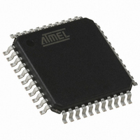
AT80C51RD2-RLRUM Atmel, AT80C51RD2-RLRUM Datasheet - Page 4

AT80C51RD2-RLRUM
Manufacturer Part Number
AT80C51RD2-RLRUM
Description
IC MCU 80C51 HI PERFORM 44VQFP
Manufacturer
Atmel
Series
80Cr
Datasheet
1.AT80C51RD2-RLRUM.pdf
(81 pages)
Specifications of AT80C51RD2-RLRUM
Core Processor
8051
Core Size
8-Bit
Speed
40MHz
Connectivity
UART/USART
Peripherals
POR, PWM, WDT
Number Of I /o
32
Program Memory Type
ROMless
Ram Size
1K x 8
Voltage - Supply (vcc/vdd)
2.7 V ~ 5.5 V
Oscillator Type
Internal
Operating Temperature
-40°C ~ 85°C
Package / Case
44-TQFP, 44-VQFP
Processor Series
AT80x
Core
8051
Data Bus Width
8 bit
Data Ram Size
1280 B
Interface Type
UART, SPI
Maximum Clock Frequency
60 MHz
Number Of Programmable I/os
32
Number Of Timers
3
Operating Supply Voltage
2.7 V to 5.5 V
Maximum Operating Temperature
+ 85 C
Mounting Style
SMD/SMT
3rd Party Development Tools
PK51, CA51, A51, ULINK2
Minimum Operating Temperature
- 40 C
Lead Free Status / RoHS Status
Lead free / RoHS Compliant
Eeprom Size
-
Program Memory Size
-
Data Converters
-
Lead Free Status / Rohs Status
Details
Available stocks
Company
Part Number
Manufacturer
Quantity
Price
Company:
Part Number:
AT80C51RD2-RLRUM
Manufacturer:
NXP
Quantity:
8 243
Table 3-1.
4
Mnemonic
V
V
P0.0 - P0.7
P1.0 - P1.7
XTAL1
XTAL2
SS
CC
AT80C51RD2
Pin Description
39 - 32
1 - 8
DIL
20
40
19
18
1
2
3
4
5
6
7
8
PLCC44
43 - 36
Pin Number
2 - 9
22
44
21
20
2
3
4
5
6
7
8
9
VQFP44 1.4
37 - 30
40 - 44
1 - 3
16
38
40
41
42
43
44
15
14
1
2
3
Type
I/O
I/O
I/O
I/O
I/O
I/O
I/O
I/O
I/O
I/O
I/O
I/O
I/O
I/O
I/O
I/O
O
I
I
I
I
I
Name and Function
Ground: 0V reference
Power Supply: This is the power supply voltage for normal, idle and power-down
operation
Port 0: Port 0 is an open-drain, bi-directional I/O port. Port 0 pins that have 1s
written to them float and can be used as high impedance inputs. Port 0 must be
polarized to V
0 is also the multiplexed low-order address and data bus during access to external
program and data memory. In this application, it uses strong internal pull-up when
emitting 1s. Port 0 also inputs the code bytes during EPROM programming.
External pull-ups are required during program verification during which P0 outputs
the code bytes.
Port 1: Port 1 is an 8-bit bi-directional I/O port with internal pull-ups. Port 1 pins
that have 1s written to them are pulled high by the internal pull-ups and can be
used as inputs. As inputs, Port 1 pins that are externally pulled low will source
current because of the internal pull-ups. Port 1 also receives the low-order address
byte during memory programming and verification.
Alternate functions for T89C51RB2/RC2 Port 1 include:
P1.0: Input/Output
T2 (P1.0): Timer/Counter 2 external count input/Clockout
P1.1: Input/Output
T2EX: Timer/Counter 2 Reload/Capture/Direction Control
P1.2: Input/Output
ECI: External Clock for the PCA
P1.3: Input/Output
CEX0: Capture/Compare External I/O for PCA module 0
P1.4: Input/Output
CEX1: Capture/Compare External I/O for PCA module 1
P1.5: Input/Output
CEX2: Capture/Compare External I/O for PCA module 2
P1.6: Input/Output
CEX3: Capture/Compare External I/O for PCA module 3
P1.7: Input/Output:
CEX4: Capture/Compare External I/O for PCA module 4
Crystal 1: Input to the inverting oscillator amplifier and input to the internal clock
generator circuits.
Crystal 2: Output from the inverting oscillator amplifier
CC
or V
SS
in order to prevent any parasitic current consumption. Port
4113D–8051–01/09


