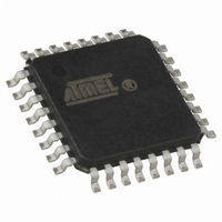
ATTINY28L-4AU Atmel, ATTINY28L-4AU Datasheet - Page 10

ATTINY28L-4AU
Manufacturer Part Number
ATTINY28L-4AU
Description
IC MCU AVR 2K FLASH 4MHZ 32-TQFP
Manufacturer
Atmel
Series
AVR® ATtinyr
Specifications of ATTINY28L-4AU
Core Processor
AVR
Core Size
8-Bit
Speed
4MHz
Peripherals
POR, WDT
Number Of I /o
11
Program Memory Size
2KB (1K x 16)
Program Memory Type
FLASH
Voltage - Supply (vcc/vdd)
2.7 V ~ 5.5 V
Oscillator Type
Internal
Operating Temperature
-40°C ~ 85°C
Package / Case
32-TQFP, 32-VQFP
Processor Series
ATTINY2x
Core
AVR8
Data Bus Width
8 bit
Data Ram Size
32 B
Maximum Clock Frequency
4 MHz
Number Of Programmable I/os
11
Number Of Timers
1
Maximum Operating Temperature
+ 85 C
Mounting Style
SMD/SMT
3rd Party Development Tools
EWAVR, EWAVR-BL
Development Tools By Supplier
ATAVRDRAGON, ATSTK500, ATSTK600, ATAVRISP2, ATAVRONEKIT
Minimum Operating Temperature
- 40 C
On-chip Adc
8 bit
Package
32TQFP
Device Core
AVR
Family Name
ATtiny
Maximum Speed
4 MHz
Ram Size
32 Byte
Operating Supply Voltage
3.3|5 V
For Use With
ATSTK600-DIP40 - STK600 SOCKET/ADAPTER 40-PDIPATSTK500 - PROGRAMMER AVR STARTER KIT
Lead Free Status / RoHS Status
Lead free / RoHS Compliant
Eeprom Size
-
Ram Size
-
Data Converters
-
Connectivity
-
Lead Free Status / Rohs Status
Details
Available stocks
Company
Part Number
Manufacturer
Quantity
Price
Memories
I/O Memory
10
ATtiny28L/V
The I/O space definition of the ATtiny28 is shown in Table 3.
Table 3. ATtiny28 I/O Space
Note:
All ATtiny28 I/O and peripherals are placed in the I/O space. The I/O locations are
accessed by the IN and OUT instructions transferring data between the 32 general-pur-
pose working registers and the I/O space. I/O registers within the address range $00 -
$1F are directly bit-accessible using the SBI and CBI instructions. In these registers, the
value of single bits can be checked by using the SBIS and SBIC instructions. Refer to
the Instruction Set section for more details.
For compatibility with future devices, reserved bits should be written to zero if accessed.
Reserved I/O memory addresses should never be written.
The I/O and peripherals control registers are explained in the following sections.
Address Hex
$3F
$1B
$1A
$19
$16
$12
$11
$10
$08
$07
$06
$05
$04
$03
$02
$01
$00
Reserved and unused locations are not shown in the table.
Name
SREG
PORTA
PACR
PINA
PINB
PORTD
DDRD
PIND
ACSR
MCUCS
ICR
IFR
TCCR0
TCNT0
MODCR
WDTCR
OSCCAL
Function
Status Register
Data Register, Port A
Port A Control Register
Input Pins, Port A
Input Pins, Port B
Data Register, Port D
Data Direction Register, Port D
Input Pins, Port D
Analog Comparator Control and Status Register
MCU Control and Status Register
Interrupt Control Register
Interrupt Flag Register
Timer/Counter0 Control Register
Timer/Counter0 (8-bit)
Modulation Control Register
Watchdog Timer Control Register
Oscillator Calibration Register
1062F–AVR–07/06


