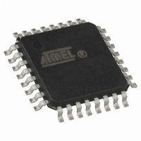
ATTINY28L-4AU Atmel, ATTINY28L-4AU Datasheet - Page 49

ATTINY28L-4AU
Manufacturer Part Number
ATTINY28L-4AU
Description
IC MCU AVR 2K FLASH 4MHZ 32-TQFP
Manufacturer
Atmel
Series
AVR® ATtinyr
Specifications of ATTINY28L-4AU
Core Processor
AVR
Core Size
8-Bit
Speed
4MHz
Peripherals
POR, WDT
Number Of I /o
11
Program Memory Size
2KB (1K x 16)
Program Memory Type
FLASH
Voltage - Supply (vcc/vdd)
2.7 V ~ 5.5 V
Oscillator Type
Internal
Operating Temperature
-40°C ~ 85°C
Package / Case
32-TQFP, 32-VQFP
Processor Series
ATTINY2x
Core
AVR8
Data Bus Width
8 bit
Data Ram Size
32 B
Maximum Clock Frequency
4 MHz
Number Of Programmable I/os
11
Number Of Timers
1
Maximum Operating Temperature
+ 85 C
Mounting Style
SMD/SMT
3rd Party Development Tools
EWAVR, EWAVR-BL
Development Tools By Supplier
ATAVRDRAGON, ATSTK500, ATSTK600, ATAVRISP2, ATAVRONEKIT
Minimum Operating Temperature
- 40 C
On-chip Adc
8 bit
Package
32TQFP
Device Core
AVR
Family Name
ATtiny
Maximum Speed
4 MHz
Ram Size
32 Byte
Operating Supply Voltage
3.3|5 V
For Use With
ATSTK600-DIP40 - STK600 SOCKET/ADAPTER 40-PDIPATSTK500 - PROGRAMMER AVR STARTER KIT
Lead Free Status / RoHS Status
Lead free / RoHS Compliant
Eeprom Size
-
Ram Size
-
Data Converters
-
Connectivity
-
Lead Free Status / Rohs Status
Details
Available stocks
Company
Part Number
Manufacturer
Quantity
Price
Chip Erase
Programming the Flash
1062F–AVR–07/06
The Chip Erase command will erase the Flash memory and the Lock bits. The Lock bits
are not reset until the Flash has been completely erased. The Fuse bits are not
changed. Chip Erase must be performed before the Flash is reprogrammed.
Load Command “Chip Erase”
1. Set XA1, XA0 to “10”. This enables command loading.
2. Set BS to “0”.
3. Set DATA to “1000 0000”. This is the command for Chip Erase.
4. Give XTAL1 a positive pulse. This loads the command.
5. Give WR a negative pulse. This starts the Chip Erase. RDY/BSY goes low.
6. Wait until RDY/BSY goes high before loading a new command.
A: Load Command “Write Flash”
1. Set XA1, XA0 to “10”. This enables command loading.
2. Set BS to “0”.
3. Set DATA to “0001 0000”. This is the command for Write Flash.
4. Give XTAL1 a positive pulse. This loads the command.
B: Load Address High Byte
1. Set XA1, XA0 to “00”. This enables address loading.
2. Set BS to “1”. This selects high byte.
3. Set DATA = Address high byte ($00 - $03).
4. Give XTAL1 a positive pulse. This loads the address high byte.
C: Load Address Low Byte
1. Set XA1, XA0 to “00”. This enables address loading.
2. Set BS to “0”. This selects low byte.
3. Set DATA = Address low byte ($00 - $FF).
4. Give XTAL1 a positive pulse. This loads the address low byte.
D: Load Data Low Byte
1. Set XA1, XA0 to “01”. This enables data loading.
2. Set DATA = Data low byte ($00 - $FF).
3. Give XTAL1 a positive pulse. This loads the data low byte.
E: Write Data Low Byte
1. Set BS to “0”. This selects low data.
2. Give WR a negative pulse. This starts programming of the data byte. RDY/BSY
3. Wait until RDY/BSY goes high to program the next byte.
(See Figure 38 for signal waveforms.)
F: Load Data High Byte
1. Set XA1, XA0 to “01”. This enables data loading.
2. Set DATA = Data high byte ($00 - $FF).
3. Give XTAL1 a positive pulse. This loads the data high byte.
G: Write Data High Byte
goes low.
ATtiny28L/V
49


