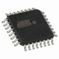
ATTINY28L-4AU Atmel, ATTINY28L-4AU Datasheet - Page 5

ATTINY28L-4AU
Manufacturer Part Number
ATTINY28L-4AU
Description
IC MCU AVR 2K FLASH 4MHZ 32-TQFP
Manufacturer
Atmel
Series
AVR® ATtinyr
Specifications of ATTINY28L-4AU
Core Processor
AVR
Core Size
8-Bit
Speed
4MHz
Peripherals
POR, WDT
Number Of I /o
11
Program Memory Size
2KB (1K x 16)
Program Memory Type
FLASH
Voltage - Supply (vcc/vdd)
2.7 V ~ 5.5 V
Oscillator Type
Internal
Operating Temperature
-40°C ~ 85°C
Package / Case
32-TQFP, 32-VQFP
Processor Series
ATTINY2x
Core
AVR8
Data Bus Width
8 bit
Data Ram Size
32 B
Maximum Clock Frequency
4 MHz
Number Of Programmable I/os
11
Number Of Timers
1
Maximum Operating Temperature
+ 85 C
Mounting Style
SMD/SMT
3rd Party Development Tools
EWAVR, EWAVR-BL
Development Tools By Supplier
ATAVRDRAGON, ATSTK500, ATSTK600, ATAVRISP2, ATAVRONEKIT
Minimum Operating Temperature
- 40 C
On-chip Adc
8 bit
Package
32TQFP
Device Core
AVR
Family Name
ATtiny
Maximum Speed
4 MHz
Ram Size
32 Byte
Operating Supply Voltage
3.3|5 V
For Use With
ATSTK600-DIP40 - STK600 SOCKET/ADAPTER 40-PDIPATSTK500 - PROGRAMMER AVR STARTER KIT
Lead Free Status / RoHS Status
Lead free / RoHS Compliant
Eeprom Size
-
Ram Size
-
Data Converters
-
Connectivity
-
Lead Free Status / Rohs Status
Details
Available stocks
Company
Part Number
Manufacturer
Quantity
Price
ALU – Arithmetic Logic
Unit
Subroutine and Interrupt
Hardware Stack
General-purpose
Register File
1062F–AVR–07/06
r a t e i n t e r r u p t v e c t o r i n t h e i n t e r r u p t v e c t o r t a b le a t t h e b e g i n n i n g o f t h e
program memory. The different interrupts have priority in accordance with their interrupt
vector position. The lower the interrupt vector address, the higher the priority.
The high-performance AVR ALU operates in direct connection with all the 32 general-
purpose working registers. Within a single clock cycle, ALU operations between regis-
ters in the register file are executed. The ALU operations are divided into three main
categories – arithmetic, logic and bit functions. Some microcontrollers in the AVR prod-
uct family feature a hardware multiplier in the arithmetic part of the ALU.
The ATtiny28 uses a 3-level-deep hardware stack for subroutines and interrupts. The
hardware stack is 10 bits wide and stores the program counter (PC) return address
while subroutines and interrupts are executed.
RCALL instructions and interrupts push the PC return address onto stack level 0, and
the data in the other stack levels 1 - 2 are pushed one level deeper in the stack. When a
RET or RETI instruction is executed the returning PC is fetched from stack level 0, and
the data in the other stack levels 1 - 2 are popped one level in the stack.
If more than three subsequent subroutine calls or interrupts are executed, the first val-
ues written to the stack are overwritten.
Figure 4 shows the structure of the 32 general-purpose registers in the CPU.
Figure 4. AVR CPU General-purpose Working Registers
All the register operating instructions in the instruction set have direct and single cycle
access to all registers. The only exception are the five constant arithmetic and logic
instructions SBCI, SUBI, CPI, ANDI and ORI between a constant and a register and the
LDI instruction for load immediate constant data. These instructions apply to the second
half of the registers in the register file – R16..R31. The general SBC, SUB, CP, AND,
OR and all other operations between two registers or on a single register apply to the
entire register file.
Registers 30 and 31 form a 16-bit pointer (the Z-pointer), which is used for indirect Flash
memory and register file access. When the register file is accessed, the contents of R31
are discarded by the CPU.
Registers
Purpose
Working
General
7
R30 (Z-Register low byte)
R31(Z-Register high byte)
R29
R28
R0
R1
R2
…
…
ATtiny28L/V
0
5


