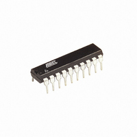
ATTINY26-16PU Atmel, ATTINY26-16PU Datasheet - Page 123

ATTINY26-16PU
Manufacturer Part Number
ATTINY26-16PU
Description
IC AVR MCU 2K 16MHZ IND 20-DIP
Manufacturer
Atmel
Series
AVR® ATtinyr
Specifications of ATTINY26-16PU
Core Processor
AVR
Core Size
8-Bit
Speed
16MHz
Connectivity
USI
Peripherals
Brown-out Detect/Reset, POR, PWM, WDT
Number Of I /o
16
Program Memory Size
2KB (1K x 16)
Program Memory Type
FLASH
Eeprom Size
128 x 8
Ram Size
128 x 8
Voltage - Supply (vcc/vdd)
4.5 V ~ 5.5 V
Data Converters
A/D 11x10b
Oscillator Type
Internal
Operating Temperature
-40°C ~ 85°C
Package / Case
20-DIP (0.300", 7.62mm)
Processor Series
ATTINY2x
Core
AVR8
Data Bus Width
8 bit
Data Ram Size
128 B
Interface Type
2-Wire/ISP/SM-Bus/SPI/UART/USI
Maximum Clock Frequency
16 MHz
Number Of Programmable I/os
16
Number Of Timers
2
Operating Supply Voltage
4.5 V to 5.5 V
Maximum Operating Temperature
+ 85 C
Mounting Style
Through Hole
3rd Party Development Tools
EWAVR, EWAVR-BL
Development Tools By Supplier
ATAVRDRAGON, ATSTK500, ATSTK600, ATAVRISP2, ATAVRONEKIT
Minimum Operating Temperature
- 40 C
On-chip Adc
11-ch x 10-bit
Package
20PDIP
Device Core
AVR
Family Name
ATtiny
Maximum Speed
16 MHz
For Use With
ATSTK600 - DEV KIT FOR AVR/AVR32770-1007 - ISP 4PORT ATMEL AVR MCU SPI/JTAGATAVRISP2 - PROGRAMMER AVR IN SYSTEMATSTK505 - ADAPTER KIT FOR 14PIN AVR MCU
Lead Free Status / RoHS Status
Lead free / RoHS Compliant
- Current page: 123 of 182
- Download datasheet (3Mb)
Data Polling Flash
Data Polling EEPROM
1477K–AVR–08/10
When a page is being programmed into the Flash, reading an address location within the page
being programmed will give the value $FF. At the time the device is ready for a new page, the
programmed value will read correctly. This is used to determine when the next page can be writ-
ten. Note that the entire page is written simultaneously and any address within the page can be
used for polling. Data polling of the Flash will not work for the value $FF, so when programming
this value, the user will have to wait for at least t
a chip-erased device contains $FF in all locations, programming of addresses that are meant to
contain $FF, can be skipped. See Table 60 for t
When a new byte has been written and is being programmed into EEPROM, reading the
address location being programmed will give the value $FF. At the time the device is ready for a
new byte, the programmed value will read correctly. This is used to determine when the next
byte can be written. This will not work for the value $FF, but the user should have the following in
mind: As a chip-erased device contains $FF in all locations, programming of addresses that are
meant to contain $FF, can be skipped. This does not apply if the EEPROM is re-programmed
without chip-erasing the device. In this case, data polling cannot be used for the value $FF, and
the user will have to wait at least t
t
Table 60. Minimum Wait Delay before Writing the Next Flash or EEPROM Location
Figure 68. Serial Programming Waveforms
WD_EEPROM
Symbol
t
t
t
t
WD_FLASH
WD_EEPROM
WD_ERASE
WD_FUSE
value.
SERIAL DATA OUTPUT
SERIAL CLOCK INPUT
SERIAL DATA INPUT
SAMPLE
(MOSI)
(MISO)
(SCK)
Minimum Wait Delay
4.5 ms
9.0 ms
9.0 ms
4.5 ms
WD_EEPROM
MSB
MSB
before programming the next byte. See Table 60 for
WD_FLASH
WD_FLASH
value.
before programming the next page. As
LSB
LSB
123
Related parts for ATTINY26-16PU
Image
Part Number
Description
Manufacturer
Datasheet
Request
R

Part Number:
Description:
Manufacturer:
Atmel Corporation
Datasheet:

Part Number:
Description:
IC AVR MCU 2K 16MHZ IND 32-QFN
Manufacturer:
Atmel
Datasheet:

Part Number:
Description:
IC AVR MCU 2K 16MHZ IND 20-SOIC
Manufacturer:
Atmel
Datasheet:

Part Number:
Description:
IC AVR MCU 2K 16MHZ IND 32-QFN
Manufacturer:
Atmel
Datasheet:

Part Number:
Description:
IC AVR MCU 2K 16MHZ IND 20-DIP
Manufacturer:
Atmel
Datasheet:

Part Number:
Description:
IC AVR MCU 2K 16MHZ COM 20-SOIC
Manufacturer:
Atmel
Datasheet:

Part Number:
Description:
IC AVR MCU 2K 16MHZ IND 20-SOIC
Manufacturer:
Atmel
Datasheet:

Part Number:
Description:
ID MCU AVR 2K 5V 16MHZ 32-QFN
Manufacturer:
Atmel
Datasheet:

Part Number:
Description:
Microcontrollers (MCU) AVR 2K FLASH 128B EE 128B SRAM ADC
Manufacturer:
Atmel
Datasheet:

Part Number:
Description:
IC AVR MCU 2K 16MHZ COM 32-QFN
Manufacturer:
Atmel
Datasheet:

Part Number:
Description:
IC AVR MCU 2K 16MHZ COM 20-DIP
Manufacturer:
Atmel
Datasheet:

Part Number:
Description:
ID MCU AVR 2K 5V 16MHZ 20-DIP
Manufacturer:
Atmel
Datasheet:

Part Number:
Description:
ID MCU AVR 2K 5V 16MHZ 20-SOIC
Manufacturer:
Atmel
Datasheet:

Part Number:
Description:
IC MCU AVR 2K 16MHZ IND 20SOIC
Manufacturer:
Atmel
Datasheet:


