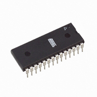
ATMEGA8A-PU Atmel, ATMEGA8A-PU Datasheet - Page 111

ATMEGA8A-PU
Manufacturer Part Number
ATMEGA8A-PU
Description
MCU AVR 8K FLASH 16MHZ 28-PDIP
Manufacturer
Atmel
Series
AVR® ATmegar
Specifications of ATMEGA8A-PU
Core Processor
AVR
Core Size
8-Bit
Speed
16MHz
Connectivity
I²C, SPI, UART/USART
Peripherals
Brown-out Detect/Reset, POR, PWM, WDT
Number Of I /o
23
Program Memory Size
8KB (4K x 16)
Program Memory Type
FLASH
Eeprom Size
512 x 8
Ram Size
1K x 8
Voltage - Supply (vcc/vdd)
2.7 V ~ 5.5 V
Data Converters
A/D 6x10b
Oscillator Type
Internal
Operating Temperature
-40°C ~ 85°C
Package / Case
28-DIP (0.300", 7.62mm)
Processor Series
ATMEGA8x
Core
AVR8
Data Bus Width
8 bit
Data Ram Size
1 KB
Interface Type
SPI, TWI, USART
Maximum Clock Frequency
16 MHz
Number Of Programmable I/os
23
Number Of Timers
3
Maximum Operating Temperature
+ 85 C
Mounting Style
Through Hole
3rd Party Development Tools
EWAVR, EWAVR-BL
Development Tools By Supplier
ATAVRDRAGON, ATSTK500, ATSTK600, ATAVRISP2, ATAVRONEKIT
Minimum Operating Temperature
- 40 C
On-chip Adc
10 bit, 6 Channel
Package
28PDIP
Device Core
AVR
Family Name
ATmega
Maximum Speed
16 MHz
Operating Supply Voltage
3.3|5 V
Controller Family/series
AVR MEGA
No. Of I/o's
23
Eeprom Memory Size
512Byte
Ram Memory Size
1KB
Cpu Speed
16MHz
Rohs Compliant
Yes
For Use With
ATSTK600 - DEV KIT FOR AVR/AVR32ATSTK500 - PROGRAMMER AVR STARTER KIT
Lead Free Status / RoHS Status
Lead free / RoHS Compliant
Available stocks
Company
Part Number
Manufacturer
Quantity
Price
Part Number:
ATMEGA8A-PU
Manufacturer:
ATMEL/爱特梅尔
Quantity:
20 000
- Current page: 111 of 308
- Download datasheet (6Mb)
17.5.3
17.6
8159D–AVR–02/11
Compare Match Output Unit
Using the Output Compare Unit
Since writing TCNT2 in any mode of operation will block all compare matches for one timer clock
cycle, there are risks involved when changing TCNT2 when using the Output Compare channel,
independently of whether the Timer/Counter is running or not. If the value written to TCNT2
equals the OCR2 value, the Compare Match will be missed, resulting in incorrect waveform gen-
eration. Similarly, do not write the TCNT2 value equal to BOTTOM when the counter is
downcounting.
The setup of the OC2 should be performed before setting the Data Direction Register for the port
pin to output. The easiest way of setting the OC2 value is to use the Force Output Compare
(FOC2) strobe bit in Normal mode. The OC2 Register keeps its value even when changing
between waveform generation modes.
Be aware that the COM21:0 bits are not double buffered together with the compare value.
Changing the COM21:0 bits will take effect immediately.
The Compare Output mode (COM21:0) bits have two functions. The waveform generator uses
the COM21:0 bits for defining the Output Compare (OC2) state at the next Compare Match.
Also, the COM21:0 bits control the OC2 pin output source.
matic of the logic affected by the COM21:0 bit setting. The I/O Registers, I/O bits, and I/O pins in
the figure are shown in bold. Only the parts of the general I/O Port Control Registers (DDR and
PORT) that are affected by the COM21:0 bits are shown. When referring to the OC2 state, the
reference is for the internal OC2 Register, not the OC2 pin.
Figure 17-4. Compare Match Output Unit, Schematic
COMn1
COMn0
FOCn
clk
I/O
Waveform
Generator
D
D
D
PORT
DDR
OCn
Q
Q
Q
Figure 17-4
1
0
shows a simplified sche-
ATmega8A
OCn
Pin
111
Related parts for ATMEGA8A-PU
Image
Part Number
Description
Manufacturer
Datasheet
Request
R

Part Number:
Description:
IC AVR MCU 8K 16MHZ 5V 32TQFP
Manufacturer:
Atmel
Datasheet:

Part Number:
Description:
IC AVR MCU 8K 16MHZ 5V 32-QFN
Manufacturer:
Atmel
Datasheet:

Part Number:
Description:
IC AVR MCU 8K 16MHZ 5V 28DIP
Manufacturer:
Atmel
Datasheet:

Part Number:
Description:
IC AVR MCU 8K 16MHZ COM 32-TQFP
Manufacturer:
Atmel
Datasheet:

Part Number:
Description:
IC AVR MCU 8K 16MHZ IND 32-TQFP
Manufacturer:
Atmel
Datasheet:

Part Number:
Description:
IC AVR MCU 8K 16MHZ COM 28-DIP
Manufacturer:
Atmel
Datasheet:

Part Number:
Description:
IC AVR MCU 8K 16MHZ IND 28-DIP
Manufacturer:
Atmel
Datasheet:

Part Number:
Description:
IC AVR MCU 8K 16MHZ COM 32-QFN
Manufacturer:
Atmel
Datasheet:

Part Number:
Description:
MCU AVR 8KB FLASH 16MHZ 32QFN
Manufacturer:
Atmel
Datasheet:

Part Number:
Description:
IC AVR MCU 8K 16MHZ IND 32-QFN
Manufacturer:
Atmel
Datasheet:

Part Number:
Description:
IC MCU AVR 8K 5V 16MHZ 32-TQFP
Manufacturer:
Atmel
Datasheet:

Part Number:
Description:
IC MCU AVR 8K 5V 16MHZ 32-QFN
Manufacturer:
Atmel
Datasheet:

Part Number:
Description:
IC MCU AVR 8K 5V 16MHZ 28-DIP
Manufacturer:
Atmel
Datasheet:


