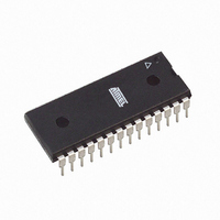
ATMEGA8A-PU Atmel, ATMEGA8A-PU Datasheet - Page 18

ATMEGA8A-PU
Manufacturer Part Number
ATMEGA8A-PU
Description
MCU AVR 8K FLASH 16MHZ 28-PDIP
Manufacturer
Atmel
Series
AVR® ATmegar
Specifications of ATMEGA8A-PU
Core Processor
AVR
Core Size
8-Bit
Speed
16MHz
Connectivity
I²C, SPI, UART/USART
Peripherals
Brown-out Detect/Reset, POR, PWM, WDT
Number Of I /o
23
Program Memory Size
8KB (4K x 16)
Program Memory Type
FLASH
Eeprom Size
512 x 8
Ram Size
1K x 8
Voltage - Supply (vcc/vdd)
2.7 V ~ 5.5 V
Data Converters
A/D 6x10b
Oscillator Type
Internal
Operating Temperature
-40°C ~ 85°C
Package / Case
28-DIP (0.300", 7.62mm)
Processor Series
ATMEGA8x
Core
AVR8
Data Bus Width
8 bit
Data Ram Size
1 KB
Interface Type
SPI, TWI, USART
Maximum Clock Frequency
16 MHz
Number Of Programmable I/os
23
Number Of Timers
3
Maximum Operating Temperature
+ 85 C
Mounting Style
Through Hole
3rd Party Development Tools
EWAVR, EWAVR-BL
Development Tools By Supplier
ATAVRDRAGON, ATSTK500, ATSTK600, ATAVRISP2, ATAVRONEKIT
Minimum Operating Temperature
- 40 C
On-chip Adc
10 bit, 6 Channel
Package
28PDIP
Device Core
AVR
Family Name
ATmega
Maximum Speed
16 MHz
Operating Supply Voltage
3.3|5 V
Controller Family/series
AVR MEGA
No. Of I/o's
23
Eeprom Memory Size
512Byte
Ram Memory Size
1KB
Cpu Speed
16MHz
Rohs Compliant
Yes
For Use With
ATSTK600 - DEV KIT FOR AVR/AVR32ATSTK500 - PROGRAMMER AVR STARTER KIT
Lead Free Status / RoHS Status
Lead free / RoHS Compliant
Available stocks
Company
Part Number
Manufacturer
Quantity
Price
Part Number:
ATMEGA8A-PU
Manufacturer:
ATMEL/爱特梅尔
Quantity:
20 000
- Current page: 18 of 308
- Download datasheet (6Mb)
7.4
7.4.1
7.5
8159D–AVR–02/11
EEPROM Data Memory
I/O Memory
EEPROM Read/Write Access
The Atmel
separate data space, in which single bytes can be read and written. The EEPROM has an
endurance of at least 100,000 write/erase cycles. The access between the EEPROM and the
CPU is described bellow, specifying the EEPROM Address Registers, the EEPROM Data Reg-
ister, and the EEPROM Control Register.
“Memory Programming” on page 226
in SPI- or Parallel Programming mode.
The EEPROM Access Registers are accessible in the I/O space.
The write access time for the EEPROM is given in
however, lets the user software detect when the next byte can be written. If the user code con-
tains instructions that write the EEPROM, some precautions must be taken. In heavily filtered
power supplies, V
some period of time to run at a voltage lower than specified as minimum for the clock frequency
used.
these situations.
In order to prevent unintentional EEPROM writes, a specific write procedure must be followed.
Refer to the description of the EEPROM Control Register for details on this.
When the EEPROM is read, the CPU is halted for four clock cycles before the next instruction is
executed. When the EEPROM is written, the CPU is halted for two clock cycles before the next
instruction is executed.
The I/O space definition of the ATmega8A is shown in
All ATmega8A I/Os and peripherals are placed in the I/O space. The I/O locations are accessed
by the IN and OUT instructions, transferring data between the 32 general purpose working regis-
ters and the I/O space. I/O Registers within the address range 0x00 - 0x1F are directly bit-
accessible using the SBI and CBI instructions. In these registers, the value of single bits can be
checked by using the SBIS and SBIC instructions. Refer to the instruction set section for more
details. When using the I/O specific commands IN and OUT, the I/O addresses 0x00 - 0x3F
must be used. When addressing I/O Registers as data space using LD and ST instructions,
0x20 must be added to these addresses.
For compatibility with future devices, reserved bits should be written to zero if accessed.
Reserved I/O memory addresses should never be written.
Some of the Status Flags are cleared by writing a logical one to them. Note that the CBI and SBI
instructions will operate on all bits in the I/O Register, writing a one back into any flag read as
set, thus clearing the flag. The CBI and SBI instructions work with registers 0x00 to 0x1F only.
The I/O and Peripherals Control Registers are explained in later sections.
See “Preventing EEPROM Corruption” on page 22.
®
AVR
®
ATmega8A contains 512 bytes of data EEPROM memory. It is organized as a
CC
is likely to rise or fall slowly on Power-up/down. This causes the device for
contains a detailed description on EEPROM Programming
Table 7-4
“” on page
for details on how to avoid problems in
on
page
289.
20. A self-timing function,
ATmega8A
18
Related parts for ATMEGA8A-PU
Image
Part Number
Description
Manufacturer
Datasheet
Request
R

Part Number:
Description:
IC AVR MCU 8K 16MHZ 5V 32TQFP
Manufacturer:
Atmel
Datasheet:

Part Number:
Description:
IC AVR MCU 8K 16MHZ 5V 32-QFN
Manufacturer:
Atmel
Datasheet:

Part Number:
Description:
IC AVR MCU 8K 16MHZ 5V 28DIP
Manufacturer:
Atmel
Datasheet:

Part Number:
Description:
IC AVR MCU 8K 16MHZ COM 32-TQFP
Manufacturer:
Atmel
Datasheet:

Part Number:
Description:
IC AVR MCU 8K 16MHZ IND 32-TQFP
Manufacturer:
Atmel
Datasheet:

Part Number:
Description:
IC AVR MCU 8K 16MHZ COM 28-DIP
Manufacturer:
Atmel
Datasheet:

Part Number:
Description:
IC AVR MCU 8K 16MHZ IND 28-DIP
Manufacturer:
Atmel
Datasheet:

Part Number:
Description:
IC AVR MCU 8K 16MHZ COM 32-QFN
Manufacturer:
Atmel
Datasheet:

Part Number:
Description:
MCU AVR 8KB FLASH 16MHZ 32QFN
Manufacturer:
Atmel
Datasheet:

Part Number:
Description:
IC AVR MCU 8K 16MHZ IND 32-QFN
Manufacturer:
Atmel
Datasheet:

Part Number:
Description:
IC MCU AVR 8K 5V 16MHZ 32-TQFP
Manufacturer:
Atmel
Datasheet:

Part Number:
Description:
IC MCU AVR 8K 5V 16MHZ 32-QFN
Manufacturer:
Atmel
Datasheet:

Part Number:
Description:
IC MCU AVR 8K 5V 16MHZ 28-DIP
Manufacturer:
Atmel
Datasheet:


