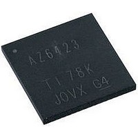
PIC18F67K22-I/MRRSL Microchip Technology, PIC18F67K22-I/MRRSL Datasheet - Page 214

PIC18F67K22-I/MRRSL
Manufacturer Part Number
PIC18F67K22-I/MRRSL
Description
MCU PIC 128K FLASH XLP 64QFN
Manufacturer
Microchip Technology
Series
PIC® XLP™ 18Fr
Datasheets
1.PIC16F722-ISS.pdf
(8 pages)
2.PIC18F65K22T-IPTRSL.pdf
(548 pages)
3.PIC18F65K22T-IPTRSL.pdf
(10 pages)
Specifications of PIC18F67K22-I/MRRSL
Core Size
8-Bit
Program Memory Size
128KB (64K x 16)
Core Processor
PIC
Speed
64MHz
Connectivity
I²C, LIN, SPI, UART/USART
Peripherals
Brown-out Detect/Reset, LVD, POR, PWM, WDT
Number Of I /o
53
Program Memory Type
FLASH
Eeprom Size
1K x 8
Ram Size
4K x 8
Voltage - Supply (vcc/vdd)
1.8 V ~ 5.5 V
Data Converters
A/D 16x12b
Oscillator Type
Internal
Operating Temperature
-40°C ~ 85°C
Package / Case
64-VFQFN, Exposed Pad
Controller Family/series
PIC18
Eeprom Memory Size
1024Byte
Ram Memory Size
3862Byte
Cpu Speed
16MIPS
No. Of Timers
11
Processor Series
PIC18F
Core
PIC
Data Bus Width
8 bit
Data Ram Size
4 KB
Interface Type
I2C, SPI, EUSART
Maximum Clock Frequency
64 MHz
Number Of Programmable I/os
53
Number Of Timers
11
Operating Supply Voltage
1.8 V to 5.5 V
Maximum Operating Temperature
+ 85 C
Mounting Style
SMD/SMT
3rd Party Development Tools
52715-96, 52716-328, 52717-734, 52712-325, EWPIC18
Development Tools By Supplier
DM180021, DM183026-2, DM183032, DV164131, MA180028
Minimum Operating Temperature
- 40 C
On-chip Adc
12 bit, 16 Channel
Lead Free Status / RoHS Status
Lead free / RoHS Compliant
Lead Free Status / RoHS Status
Lead free / RoHS Compliant
Available stocks
Company
Part Number
Manufacturer
Quantity
Price
Company:
Part Number:
PIC18F67K22-I/MRRSL
Manufacturer:
FSC
Quantity:
250
- PIC16F722-ISS PDF datasheet
- PIC18F65K22T-IPTRSL PDF datasheet #2
- PIC18F65K22T-IPTRSL PDF datasheet #3
- Current page: 214 of 548
- Download datasheet (5Mb)
PIC18F87K22 FAMILY
16.3
Timer3/5/7 can be configured for 16-bit reads and
writes (see Figure 16.3). When the RD16 control bit
(TxCON<1>) is set, the address for TMRxH is mapped
to a buffer register for the high byte of Timer3/5/7. A
read from TMRxL will load the contents of the high byte
of Timer3/5/7 into the Timerx High Byte Buffer register.
This provides users with the ability to accurately read
all 16 bits of Timer3/5/7 without having to determine
whether a read of the high byte, followed by a read of
the low byte, has become invalid due to a rollover
between reads.
A write to the high byte of Timer3/5/7 must also take
place through the TMRxH Buffer register. The Timer3/
5/7 high byte is updated with the contents of TMRxH
when a write occurs to TMRxL. This allows users to
write all 16 bits to both the high and low bytes of
Timer3/5/7 at once.
The high byte of Timer3/5/7 is not directly readable or
writable in this mode. All reads and writes must take
place through the Timerx High Byte Buffer register.
Writes to TMRxH do not clear the Timer3/5/7 prescaler.
The prescaler is only cleared on writes to TMRxL.
DS39960B-page 214
Timer3/5/7 16-Bit Read/Write Mode
Preliminary
16.4
The SOSC internal oscillator may be used as the clock
source for Timer3/5/7. The SOSC oscillator is enabled
by any peripheral that requests it. There are eight ways
the SOSC can be enabled: if the SOSC is selected as
the source by any of the odd timers, which is done by
each respective SOSCEN bit (TxCON<3>), if the
SOSC is selected as the RTCC source by the RTCOSC
Configuration bit (CONFIG3L<1>), if the SOSC is
selected as the CPU clock source by the SCS bits
(OSCCON<1:0>) or if the SOSCGO bit is set
(OSCCON2<3>). The SOSCGO bit is used to warm up
the SOSC so that it is ready before any peripheral
requests it. To use it as the Timer3/5/7 clock source, the
TMRxCS bit must also be set. As previously noted, this
also configures Timer3/5/7 to increment on every rising
edge of the oscillator source.
The SOSC oscillator is described in Section 14.5
“SOSC Oscillator”.
Using the SOSC Oscillator as the
Timer3/5/7 Clock Source
2010 Microchip Technology Inc.
Related parts for PIC18F67K22-I/MRRSL
Image
Part Number
Description
Manufacturer
Datasheet
Request
R

Part Number:
Description:
MCU PIC 128K FLASH XLP 64TQFP
Manufacturer:
Microchip Technology
Datasheet:

Part Number:
Description:
128kB Flash, 4kB RAM, 1kB EE, NanoWatt XLP, GP 64 QFN 9x9x0.9mm TUBE
Manufacturer:
Microchip Technology
Datasheet:

Part Number:
Description:
128kB Flash, 4kB RAM, 1kB EE, NanoWatt XLP, GP 64 TQFP 10x10x1mm TRAY
Manufacturer:
Microchip Technology
Datasheet:

Part Number:
Description:
128kB Flash, 4kB RAM, 1kB EE, NanoWatt XLP, GP 64 QFN 9x9x0.9mm TUBE
Manufacturer:
Microchip Technology
Datasheet:

Part Number:
Description:
128kB Flash, 4kB RAM, 1kB EE, NanoWatt XLP, GP 64 TQFP 10x10x1mm TRAY
Manufacturer:
Microchip Technology

Part Number:
Description:
Manufacturer:
Microchip Technology Inc.
Datasheet:

Part Number:
Description:
Manufacturer:
Microchip Technology Inc.
Datasheet:

Part Number:
Description:
Manufacturer:
Microchip Technology Inc.
Datasheet:

Part Number:
Description:
Manufacturer:
Microchip Technology Inc.
Datasheet:

Part Number:
Description:
Manufacturer:
Microchip Technology Inc.
Datasheet:

Part Number:
Description:
Manufacturer:
Microchip Technology Inc.
Datasheet:


