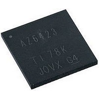
PIC18F67K22-I/MRRSL Microchip Technology, PIC18F67K22-I/MRRSL Datasheet - Page 282

PIC18F67K22-I/MRRSL
Manufacturer Part Number
PIC18F67K22-I/MRRSL
Description
MCU PIC 128K FLASH XLP 64QFN
Manufacturer
Microchip Technology
Series
PIC® XLP™ 18Fr
Datasheets
1.PIC16F722-ISS.pdf
(8 pages)
2.PIC18F65K22T-IPTRSL.pdf
(548 pages)
3.PIC18F65K22T-IPTRSL.pdf
(10 pages)
Specifications of PIC18F67K22-I/MRRSL
Core Size
8-Bit
Program Memory Size
128KB (64K x 16)
Core Processor
PIC
Speed
64MHz
Connectivity
I²C, LIN, SPI, UART/USART
Peripherals
Brown-out Detect/Reset, LVD, POR, PWM, WDT
Number Of I /o
53
Program Memory Type
FLASH
Eeprom Size
1K x 8
Ram Size
4K x 8
Voltage - Supply (vcc/vdd)
1.8 V ~ 5.5 V
Data Converters
A/D 16x12b
Oscillator Type
Internal
Operating Temperature
-40°C ~ 85°C
Package / Case
64-VFQFN, Exposed Pad
Controller Family/series
PIC18
Eeprom Memory Size
1024Byte
Ram Memory Size
3862Byte
Cpu Speed
16MIPS
No. Of Timers
11
Processor Series
PIC18F
Core
PIC
Data Bus Width
8 bit
Data Ram Size
4 KB
Interface Type
I2C, SPI, EUSART
Maximum Clock Frequency
64 MHz
Number Of Programmable I/os
53
Number Of Timers
11
Operating Supply Voltage
1.8 V to 5.5 V
Maximum Operating Temperature
+ 85 C
Mounting Style
SMD/SMT
3rd Party Development Tools
52715-96, 52716-328, 52717-734, 52712-325, EWPIC18
Development Tools By Supplier
DM180021, DM183026-2, DM183032, DV164131, MA180028
Minimum Operating Temperature
- 40 C
On-chip Adc
12 bit, 16 Channel
Lead Free Status / RoHS Status
Lead free / RoHS Compliant
Lead Free Status / RoHS Status
Lead free / RoHS Compliant
Available stocks
Company
Part Number
Manufacturer
Quantity
Price
Company:
Part Number:
PIC18F67K22-I/MRRSL
Manufacturer:
FSC
Quantity:
250
- PIC16F722-ISS PDF datasheet
- PIC18F65K22T-IPTRSL PDF datasheet #2
- PIC18F65K22T-IPTRSL PDF datasheet #3
- Current page: 282 of 548
- Download datasheet (5Mb)
PIC18F87K22 FAMILY
21.3.2
When initializing the SPI, several options need to be
specified. This is done by programming the appropriate
control bits (SSPxCON1<5:0> and SSPxSTAT<7:6>).
These control bits allow the following to be specified:
• Master mode (SCKx is the clock output)
• Slave mode (SCKx is the clock input)
• Clock Polarity (Idle state of SCKx)
• Data Input Sample Phase (middle or end of data
• Clock Edge (output data on rising/falling edge of
• Clock Rate (Master mode only)
• Slave Select mode (Slave mode only)
Each MSSP module consists of a transmit/receive shift
register (SSPxSR) and a buffer register (SSPxBUF).
The SSPxSR shifts the data in and out of the device,
MSb first. The SSPxBUF holds the data that was
written to the SSPxSR until the received data is ready.
Once the 8 bits of data have been received, that byte is
moved to the SSPxBUF register. Then, the Buffer Full
detect bit, BF (SSPxSTAT<0>) and the interrupt flag bit,
SSPxIF, are set. This double-buffering of the received
data (SSPxBUF) allows the next byte to start reception
before reading the data that was just received. Any
write to the SSPxBUF register during transmis-
sion/reception of data will be ignored and the Write
Collision Detect bit, WCOL (SSPxCON1<7>), will be
set. User software must clear the WCOL bit so that it
can be determined if the following write(s) to the
SSPxBUF register completed successfully.
EXAMPLE 21-1:
DS39960B-page 282
LOOP
output time)
SCKx)
BTFSS
BRA
MOVF
MOVWF
MOVF
MOVWF
OPERATION
SSP1STAT, BF
LOOP
SSP1BUF, W
RXDATA
TXDATA, W
SSP1BUF
LOADING THE SSP1BUF (SSP1SR) REGISTER
;Has data been received (transmit complete)?
;No
;WREG reg = contents of SSP1BUF
;Save in user RAM, if data is meaningful
;W reg = contents of TXDATA
;New data to xmit
Preliminary
When the application software is expecting to receive
valid data, the SSPxBUF should be read before the next
byte of data to transfer is written to the SSPxBUF. The
Buffer Full bit, BF (SSPxSTAT<0>), indicates when
SSPxBUF has been loaded with the received data
(transmission is complete). When the SSPxBUF is read,
the BF bit is cleared. This data may be irrelevant if the
SPI is only a transmitter. Generally, the MSSP interrupt
is used to determine when the transmission/reception
has completed. If the interrupt method is not going to be
used, then software polling can be done to ensure that a
write collision does not occur. Example 21-1 shows the
loading
transmission.
The SSPxSR is not directly readable or writable and
can only be accessed by addressing the SSPxBUF
register. Additionally, the SSPxSTAT register indicates
the various status conditions.
21.3.3
The drivers for the SDOx output and SCKx clock pins
can be optionally configured as open-drain outputs.
This feature allows the voltage level on the pin to be
pulled to a higher level through an external pull-up
resistor, and allows the output to communicate with
external circuits without the need for additional level
shifters. For more information, see Section 12.1.3
“Open-Drain Outputs”.
The open-drain output option is controlled by the
SSP2OD and SSP1OD bits (ODCON3<1:0>). Setting
an SSPxOD bit configures the SDOx and SCKx pins for
the corresponding module for open-drain operation.
Note:
of
OPEN-DRAIN OUTPUT OPTION
To avoid lost data in Master mode, a
read of the SSPxBUF must be per-
formed to clear the Buffer Full (BF)
detect bit (SSPxSTAT<0>) between
each transmission.
the
SSPxBUF
2010 Microchip Technology Inc.
(SSPxSR)
for
data
Related parts for PIC18F67K22-I/MRRSL
Image
Part Number
Description
Manufacturer
Datasheet
Request
R

Part Number:
Description:
MCU PIC 128K FLASH XLP 64TQFP
Manufacturer:
Microchip Technology
Datasheet:

Part Number:
Description:
128kB Flash, 4kB RAM, 1kB EE, NanoWatt XLP, GP 64 QFN 9x9x0.9mm TUBE
Manufacturer:
Microchip Technology
Datasheet:

Part Number:
Description:
128kB Flash, 4kB RAM, 1kB EE, NanoWatt XLP, GP 64 TQFP 10x10x1mm TRAY
Manufacturer:
Microchip Technology
Datasheet:

Part Number:
Description:
128kB Flash, 4kB RAM, 1kB EE, NanoWatt XLP, GP 64 QFN 9x9x0.9mm TUBE
Manufacturer:
Microchip Technology
Datasheet:

Part Number:
Description:
128kB Flash, 4kB RAM, 1kB EE, NanoWatt XLP, GP 64 TQFP 10x10x1mm TRAY
Manufacturer:
Microchip Technology

Part Number:
Description:
Manufacturer:
Microchip Technology Inc.
Datasheet:

Part Number:
Description:
Manufacturer:
Microchip Technology Inc.
Datasheet:

Part Number:
Description:
Manufacturer:
Microchip Technology Inc.
Datasheet:

Part Number:
Description:
Manufacturer:
Microchip Technology Inc.
Datasheet:

Part Number:
Description:
Manufacturer:
Microchip Technology Inc.
Datasheet:

Part Number:
Description:
Manufacturer:
Microchip Technology Inc.
Datasheet:


