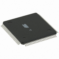
ATMEGA6490A-AU Atmel, ATMEGA6490A-AU Datasheet - Page 324

ATMEGA6490A-AU
Manufacturer Part Number
ATMEGA6490A-AU
Description
IC MCU AVR 64K FLASH 100TQFP
Manufacturer
Atmel
Series
AVR® ATmegar
Specifications of ATMEGA6490A-AU
Core Processor
AVR
Core Size
8-Bit
Speed
20MHz
Connectivity
SPI, UART/USART, USI
Peripherals
Brown-out Detect/Reset, LCD, POR, PWM, WDT
Number Of I /o
69
Program Memory Size
64KB (32K x 16)
Program Memory Type
FLASH
Eeprom Size
2K x 8
Ram Size
4K x 8
Voltage - Supply (vcc/vdd)
1.8 V ~ 5.5 V
Data Converters
A/D 8x10b
Oscillator Type
Internal
Operating Temperature
-40°C ~ 85°C
Package / Case
100-TFQFP
Processor Series
ATmega
Core
AVR
Data Bus Width
8 bit
Data Ram Size
4 KB
Interface Type
SPI, USART
Maximum Clock Frequency
20 MHz
Number Of Programmable I/os
69
Number Of Timers
3
Operating Supply Voltage
3.3 V
Maximum Operating Temperature
+ 85 C
Mounting Style
SMD/SMT
Minimum Operating Temperature
- 40 C
Operating Temperature Range
- 40 C to + 85 C
Lead Free Status / RoHS Status
Lead free / RoHS Compliant
Available stocks
Company
Part Number
Manufacturer
Quantity
Price
Company:
Part Number:
ATMEGA6490A-AU
Manufacturer:
Atmel
Quantity:
1 250
Company:
Part Number:
ATMEGA6490A-AUR
Manufacturer:
Maxim
Quantity:
43
- Current page: 324 of 712
- Download datasheet (41Mb)
27.7.13
27.7.14
27.7.15
8284A–AVR–10/10
Reading the Signature Bytes
Reading the Calibration Byte
Parallel Programming Characteristics
Figure 27-6. Mapping Between BS1, BS2 and the Fuse and Lock Bits During Read
The algorithm for reading the Signature bytes is as follows (refer to
page 317
1. A: Load Command “0000 1000”.
2. B: Load Address Low Byte (0x00 - 0x02).
3. Set OE to “0”, and BS1 to “0”. The selected Signature byte can now be read at DATA.
4. Set OE to “1”.
The algorithm for reading the Calibration byte is as follows (refer to
page 317
1. A: Load Command “0000 1000”.
2. B: Load Address Low Byte, 0x00.
3. Set OE to “0”, and BS1 to “1”. The Calibration byte can now be read at DATA.
4. Set OE to “1”.
Figure 27-7. Parallel Programming Timing, Including some General Timing Requirements
ATmega169A/169PA/329A/329PA/649A/649P/3290A/3290PA/6490A/6490P
(DATA, XA0/1, BS1, BS2)
for details on Command and Address loading):
for details on Command and Address loading):
Data & Contol
Extended Fuse Byte
Fuse Low Byte
RDY/BSY
Fuse High Byte
PAGEL
XTAL1
Lock Bits
WR
t
t
BVPH
DVXH
BS2
BS2
t
t
XHXL
PHPL
0
1
0
1
t
t
t
t
XLDX
XLWL
PLBX
PLWL
t
BVWL
BS1
t
WLWH
WLRL
0
1
”Programming the Flash” on
”Programming the Flash” on
t
WLBX
DATA
t
WLRH
324
Related parts for ATMEGA6490A-AU
Image
Part Number
Description
Manufacturer
Datasheet
Request
R

Part Number:
Description:
Manufacturer:
Atmel Corporation
Datasheet:

Part Number:
Description:
IC AVR MCU FLASH 64K 64-QFN
Manufacturer:
Atmel
Datasheet:

Part Number:
Description:
IC AVR MCU FLASH 64K 64TQFP
Manufacturer:
Atmel
Datasheet:

Part Number:
Description:
IC AVR MCU FLASH 64K 5V 64TQFP
Manufacturer:
Atmel
Datasheet:

Part Number:
Description:
IC AVR MCU FLASH 64K 5V 64QFN
Manufacturer:
Atmel
Datasheet:

Part Number:
Description:
MCU AVR 64KB FLASH 16MHZ 64QFN
Manufacturer:
Atmel
Datasheet:

Part Number:
Description:
IC MCU AVR FLASH 64K 64TQFP
Manufacturer:
Atmel
Datasheet:

Part Number:
Description:
Manufacturer:
Atmel Corporation
Datasheet:

Part Number:
Description:
Manufacturer:
ATMEL Corporation
Datasheet:

Part Number:
Description:
Manufacturer:
ATMEL Corporation
Datasheet:

Part Number:
Description:
IC AVR MCU 64K 16MHZ 5V 64TQFP
Manufacturer:
Atmel
Datasheet:

Part Number:
Description:
IC AVR MCU 64K 16MHZ 5V 64-QFN
Manufacturer:
Atmel
Datasheet:

Part Number:
Description:
IC AVR MCU 64K 16MHZ COM 64-TQFP
Manufacturer:
Atmel
Datasheet:

Part Number:
Description:
IC AVR MCU 64K 16MHZ IND 64-TQFP
Manufacturer:
Atmel
Datasheet:

Part Number:
Description:
IC AVR MCU 64K 16MHZ COM 64-QFN
Manufacturer:
Atmel
Datasheet:


