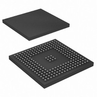
AT91SAM9XE256-CU Atmel, AT91SAM9XE256-CU Datasheet - Page 145

AT91SAM9XE256-CU
Manufacturer Part Number
AT91SAM9XE256-CU
Description
MCU ARM9 256K FLASH 217-BGA
Manufacturer
Atmel
Series
AT91SAMr
Specifications of AT91SAM9XE256-CU
Core Processor
ARM9
Core Size
16/32-Bit
Speed
180MHz
Connectivity
EBI/EMI, Ethernet, I²C, MMC, SPI, SSC, UART/USART, USB
Peripherals
Brown-out Detect/Reset, POR, PWM, WDT
Number Of I /o
96
Program Memory Size
256KB (256K x 8)
Program Memory Type
FLASH
Ram Size
56K x 8
Voltage - Supply (vcc/vdd)
1.65 V ~ 1.95 V
Data Converters
A/D 4x10b
Oscillator Type
Internal
Operating Temperature
-40°C ~ 85°C
Package / Case
217-LFBGA
Processor Series
AT91SAMx
Core
ARM926EJ-S
Data Bus Width
32 bit
Data Ram Size
32 KB
Interface Type
2-Wire, EBI, I2S, SPI, USART
Maximum Clock Frequency
180 MHz
Number Of Programmable I/os
96
Number Of Timers
6
Maximum Operating Temperature
+ 85 C
Mounting Style
SMD/SMT
3rd Party Development Tools
JTRACE-ARM-2M, KSK-AT91SAM9XE-PL, MDK-ARM, RL-ARM, ULINK2
Development Tools By Supplier
AT91SAM-ICE, AT91-ISP, AT91SAM9XE-EK
Minimum Operating Temperature
- 40 C
On-chip Adc
10 bit, 4 Channel
Package
217LFBGA
Device Core
ARM926EJ-S
Family Name
91S
Maximum Speed
180 MHz
Operating Supply Voltage
1.8|2.5|3.3 V
For Use With
AT91SAM9XE-EK - KIT EVAL FOR AT91SAM9XEAT91SAM-ICE - EMULATOR FOR AT91 ARM7/ARM9
Lead Free Status / RoHS Status
Lead free / RoHS Compliant
Eeprom Size
-
Lead Free Status / Rohs Status
Lead free / RoHS Compliant
Available stocks
Company
Part Number
Manufacturer
Quantity
Price
Company:
Part Number:
AT91SAM9XE256-CU
Manufacturer:
ATMEL
Quantity:
215
- Current page: 145 of 860
- Download datasheet (13Mb)
20.3.2
20.3.2.1
Figure 20-2. Code Read Optimization in ARM Mode for FWS = 0
Note:
6254C–ATARM–22-Jan-10
Buffer 0 (128bits)
Buffer 1 (128bits)
Data To ARM
ARM Request
Flash Access
Master Clock
(32-bit)
When FWS is equal to 0, all the accesses are performed in a single-cycle access.
Read Operations
Code Read Optimization
@Byte 0
XXX
XXX
Bytes 0-15
An optimized controller manages embedded Flash reads, thus increasing performance when the
processor is running in ARM and Thumb mode by means of the 128-bit wide memory interface.
The Flash memory is accessible through 8-, 16- and 32-bit reads.
As the Flash block size is smaller than the address space reserved for the internal memory area,
the embedded Flash wraps around the address space and appears to be repeated within it.
The read operations can be performed with or without wait states. Wait states must be pro-
grammed in the field FWS (Flash Read Wait State) in the Flash Mode Register (EEFC_FMR).
Defining FWS to be 0 enables the single-cycle access of the embedded Flash. Refer to the Elec-
trical Characteristics for more details.
A system of 2 x 128-bit buffers is added in order to optimize sequential Code Fetch.
Note:
@Byte 4
Bytes 0-3
XXX
Immediate consecutive code read accesses are not mandatory to benefit from this optimization.
Bytes 16-31
@Byte 8
Bytes 4-7
AT91SAM9XE128/256/512 Preliminary
@Byte 12
Bytes 8-11
Bytes 0-15
@Byte 16
Bytes 12-15
Bytes 32-47
@Byte 20
Bytes 16-19
Bytes 16-31
@Byte 24
Bytes 20-23
Bytes 24-27
@Byte 28
Bytes 32-47
@Byte 32
Bytes 28-31
145
Related parts for AT91SAM9XE256-CU
Image
Part Number
Description
Manufacturer
Datasheet
Request
R

Part Number:
Description:
KIT EVAL FOR AT91SAM9XE
Manufacturer:
Atmel
Datasheet:

Part Number:
Description:
MCU ARM9 64K SRAM 144-LFBGA
Manufacturer:
Atmel
Datasheet:

Part Number:
Description:
IC ARM7 MCU FLASH 256K 100LQFP
Manufacturer:
Atmel
Datasheet:

Part Number:
Description:
IC ARM9 MPU 217-LFBGA
Manufacturer:
Atmel
Datasheet:

Part Number:
Description:
MCU ARM9 ULTRA LOW PWR 217-LFBGA
Manufacturer:
Atmel
Datasheet:

Part Number:
Description:
MCU ARM9 324-TFBGA
Manufacturer:
Atmel
Datasheet:

Part Number:
Description:
IC MCU ARM9 SAMPLING 217CBGA
Manufacturer:
Atmel
Datasheet:

Part Number:
Description:
IC ARM9 MCU 217-LFBGA
Manufacturer:
Atmel
Datasheet:

Part Number:
Description:
IC ARM9 MCU 208-PQFP
Manufacturer:
Atmel
Datasheet:

Part Number:
Description:
MCU ARM 512K HS FLASH 100-LQFP
Manufacturer:
Atmel
Datasheet:

Part Number:
Description:
MCU ARM 512K HS FLASH 100-TFBGA
Manufacturer:
Atmel
Datasheet:

Part Number:
Description:
IC ARM9 MCU 200 MHZ 324-TFBGA
Manufacturer:
Atmel
Datasheet:

Part Number:
Description:
IC ARM MCU 16BIT 128K 256BGA
Manufacturer:
Atmel
Datasheet:

Part Number:
Description:
IC ARM7 MCU 32BIT 128K 64LQFP
Manufacturer:
Atmel
Datasheet:

Part Number:
Description:
IC ARM7 MCU FLASH 256K 128-LQFP
Manufacturer:
Atmel
Datasheet:


