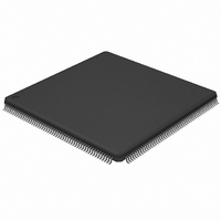
LPC2420FBD208,551 NXP Semiconductors, LPC2420FBD208,551 Datasheet - Page 17

LPC2420FBD208,551
Manufacturer Part Number
LPC2420FBD208,551
Description
IC ARM7 MCU ROMLESS 208LQFP
Manufacturer
NXP Semiconductors
Series
LPC2400r
Datasheet
1.LPC2460FBD208551.pdf
(79 pages)
Specifications of LPC2420FBD208,551
Program Memory Type
ROMless
Package / Case
208-LQFP
Core Processor
ARM7
Core Size
16/32-Bit
Speed
72MHz
Connectivity
EBI/EMI, I²C, Microwire, MMC, SPI, SSI, SSP, UART/USART, USB OTG
Peripherals
Brown-out Detect/Reset, DMA, I²S, POR, PWM, WDT
Number Of I /o
160
Ram Size
82K x 8
Voltage - Supply (vcc/vdd)
3 V ~ 3.6 V
Data Converters
A/D 8x10b; D/A 1x10b
Oscillator Type
Internal
Operating Temperature
-40°C ~ 85°C
Processor Series
LPC24
Core
ARM7TDMI-S
Data Bus Width
16 bit, 32 bit
Data Ram Size
82 KB
Interface Type
CAN/I2C/I2S/SPI/SSP/UART/USB
Maximum Clock Frequency
72 MHz
Number Of Programmable I/os
160
Number Of Timers
4
Operating Supply Voltage
3.3 V
Maximum Operating Temperature
+ 85 C
Mounting Style
SMD/SMT
3rd Party Development Tools
MDK-ARM, RL-ARM, ULINK2
Minimum Operating Temperature
- 40 C
On-chip Adc
8-ch x 10-bit
On-chip Dac
1-ch x 10-bit
Lead Free Status / RoHS Status
Lead free / RoHS Compliant
Eeprom Size
-
Program Memory Size
-
Lead Free Status / Rohs Status
Lead free / RoHS Compliant
Other names
568-4527
935286745551
935286745551
Available stocks
Company
Part Number
Manufacturer
Quantity
Price
Company:
Part Number:
LPC2420FBD208,551
Manufacturer:
NXP Semiconductors
Quantity:
10 000
NXP Semiconductors
Table 4.
LPC2420_60_5
Preliminary data sheet
Symbol
P2[9]/
USB_CONNECT1/
RXD2/
EXTIN0
P2[10]/EINT0
P2[11]/EINT1/
MCIDAT1/
I2STX_CLK
P2[12]/EINT2/
MCIDAT2/
I2STX_WS
P2[13]/EINT3/
MCIDAT3/
I2STX_SDA
P2[14]/CS2/
CAP2[0]/SDA1
P2[15]/CS3/
CAP2[1]/SCL1
P2[16]/CAS
P2[17]/RAS
P2[18]/
CLKOUT0
P2[19]/
CLKOUT1
Pin description
Pin
132
110
108
106
102
91
99
87
95
59
67
[6]
[6]
[1]
[1]
[1]
[1]
[6]
[1]
[6]
[6]
[6]
…continued
Ball
H16
N15
T17
N14
T16
R12
P13
R11
R13
U3
R7
[1]
[1]
[6]
[6]
[6]
[1]
[1]
[6]
[6]
[6]
[1]
Type
I/O
O
I
I
I/O
I
I/O
I
I/O
I/O
I/O
I
I/O
I/O
I/O
I
I/O
I/O
I/O
O
I
I/O
I/O
O
I
I/O
I/O
O
I/O
O
I/O
O
I/O
O
Rev. 05 — 24 February 2010
Description
P2[9] — General purpose digital input/output pin.
USB_CONNECT1 — USB1 SoftConnect control. Signal used to switch
an external 1.5 kΩ resistor under the software control. Used with the
SoftConnect USB feature.
RXD2 — Receiver input for UART2.
EXTIN0 — External Trigger Input.
P2[10] — General purpose digital input/output pin.
Note: LOW on this pin while RESET is LOW forces on-chip bootloader to
take over control of the part after a reset.
EINT0 — External interrupt 0 input.
P2[11] — General purpose digital input/output pin.
EINT1 — External interrupt 1 input.
MCIDAT1 — Data line 1 for SD/MMC interface.
I2STX_CLK — Transmit Clock. It is driven by the master and received by
the slave. Corresponds to the signal SCK in the I
P2[12] — General purpose digital input/output pin.
EINT2 — External interrupt 2 input.
MCIDAT2 — Data line 2 for SD/MMC interface.
I2STX_WS — Transmit Word Select. It is driven by the master and
received by the slave. Corresponds to the signal WS in the I
specification.
P2[13] — General purpose digital input/output pin.
EINT3 — External interrupt 3 input.
MCIDAT3 — Data line 3 for SD/MMC interface.
I2STX_SDA — Transmit data. It is driven by the transmitter and read by
the receiver. Corresponds to the signal SD in the I
P2[14] — General purpose digital input/output pin.
CS2 — LOW active Chip Select 2 signal.
CAP2[0] — Capture input for Timer 2, channel 0.
SDA1 — I
P2[15] — General purpose digital input/output pin.
CS3 — LOW active Chip Select 3 signal.
CAP2[1] — Capture input for Timer 2, channel 1.
SCL1 — I
P2[16] — General purpose digital input/output pin.
CAS — LOW active SDRAM Column Address Strobe.
P2[17] — General purpose digital input/output pin.
RAS — LOW active SDRAM Row Address Strobe.
P2[18] — General purpose digital input/output pin.
CLKOUT0 — SDRAM clock 0.
P2[19] — General purpose digital input/output pin.
CLKOUT1 — SDRAM clock 1.
2
2
C1 clock input/output (this is not an open-drain pin).
C1 data input/output (this is not an open-drain pin).
Flashless 16-bit/32-bit microcontroller
LPC2420/2460
2
S-bus specification.
2
S-bus specification.
© NXP B.V. 2010. All rights reserved.
2
S-bus
17 of 79


