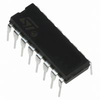
ST7FLIT15BY0B6 STMicroelectronics, ST7FLIT15BY0B6 Datasheet - Page 63

ST7FLIT15BY0B6
Manufacturer Part Number
ST7FLIT15BY0B6
Description
IC MCU 8BIT 2K FLASH 16-DIP
Manufacturer
STMicroelectronics
Series
ST7r
Datasheet
1.ST7FLIT15BY1M6.pdf
(159 pages)
Specifications of ST7FLIT15BY0B6
Core Processor
ST7
Core Size
8-Bit
Speed
8MHz
Connectivity
SPI
Peripherals
LVD, POR, PWM, WDT
Number Of I /o
11
Program Memory Size
2KB (2K x 8)
Program Memory Type
FLASH
Ram Size
256 x 8
Voltage - Supply (vcc/vdd)
2.7 V ~ 5.5 V
Data Converters
A/D 7x10b
Oscillator Type
Internal
Operating Temperature
-40°C ~ 85°C
Package / Case
16-DIP (0.300", 7.62mm)
Processor Series
ST7FLIT1x
Core
ST7
Data Bus Width
8 bit
Data Ram Size
256 B
Interface Type
SPI
Maximum Clock Frequency
8 MHz
Number Of Programmable I/os
17
Number Of Timers
4
Maximum Operating Temperature
+ 85 C
Mounting Style
Through Hole
Development Tools By Supplier
ST7FLITE-SK/RAIS, ST7MDT10-DVP3, ST7MDT10-EMU3, STX-RLINK
Minimum Operating Temperature
- 40 C
On-chip Adc
10 bit, 7 Channel
For Use With
497-8427 - BOARD DEMO USB LI-ION ST7260E2497-5049 - KIT STARTER RAISONANCE ST7FLITE
Lead Free Status / RoHS Status
Lead free / RoHS Compliant
Eeprom Size
-
Lead Free Status / Rohs Status
Details
- Current page: 63 of 159
- Download datasheet (3Mb)
DUAL 12-BIT AUTORELOAD TIMER 4 (Cont’d)
11.2.3.4 Output Compare Mode
To use this function, load a 12-bit value in the
Preload DCRxH and DCRxL registers.
When the 12-bit upcounter CNTR1 reaches the
value stored in the Active DCRxH and DCRxL reg-
isters, the CMPFx bit in the PWMxCSR register is
set and an interrupt request is generated if the
CMPIE bit is set.
In single Timer mode the output compare function
is performed only on CNTR1. The difference be-
tween both the modes is that, in Single Timer
mode, CNTR1 can be compared with any of the
four DCR registers, and in Dual Timer mode,
Figure 42. Block Diagram of Output Compare Mode (single timer)
(ATCSR2)
(ATCSR)
TRAN1
OVF
DCRx
PRELOAD DUTY CYCLE REG0/1/2/3
CNTR1
ACTIVE DUTY CYCLE REGx
COUNTER 1
CMP
INTERRUPT
CNTR1 is compared with DCR0 or DCR1 and
CNTR2 is compared with DCR2 or DCR3.
Notes:
1. The output compare function is only available
for DCRx values other than 0 (reset value).
2. Duty cycle registers are buffered internally. The
CPU writes in Preload Duty Cycle Registers and
these values are transferred in Active Duty Cycle
Registers after an overflow event if the corre-
sponding transfer bit (TRANx bit) is set. Output
compare is done by comparing these active DCRx
values with the counters.
OUTPUT COMPARE CIRCUIT
REQUEST
CMPIE
CMPFx (PWMxCSR)
(ATCSR)
ST7LITE1xB
63/159
1
Related parts for ST7FLIT15BY0B6
Image
Part Number
Description
Manufacturer
Datasheet
Request
R

Part Number:
Description:
STMicroelectronics [RIPPLE-CARRY BINARY COUNTER/DIVIDERS]
Manufacturer:
STMicroelectronics
Datasheet:

Part Number:
Description:
STMicroelectronics [LIQUID-CRYSTAL DISPLAY DRIVERS]
Manufacturer:
STMicroelectronics
Datasheet:

Part Number:
Description:
BOARD EVAL FOR MEMS SENSORS
Manufacturer:
STMicroelectronics
Datasheet:

Part Number:
Description:
NPN TRANSISTOR POWER MODULE
Manufacturer:
STMicroelectronics
Datasheet:

Part Number:
Description:
TURBOSWITCH ULTRA-FAST HIGH VOLTAGE DIODE
Manufacturer:
STMicroelectronics
Datasheet:

Part Number:
Description:
Manufacturer:
STMicroelectronics
Datasheet:

Part Number:
Description:
DIODE / SCR MODULE
Manufacturer:
STMicroelectronics
Datasheet:

Part Number:
Description:
DIODE / SCR MODULE
Manufacturer:
STMicroelectronics
Datasheet:

Part Number:
Description:
Search -----> STE16N100
Manufacturer:
STMicroelectronics
Datasheet:

Part Number:
Description:
Search ---> STE53NA50
Manufacturer:
STMicroelectronics
Datasheet:

Part Number:
Description:
NPN Transistor Power Module
Manufacturer:
STMicroelectronics
Datasheet:

Part Number:
Description:
DIODE / SCR MODULE
Manufacturer:
STMicroelectronics
Datasheet:


