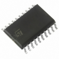
ST7FLITE35F2M6 STMicroelectronics, ST7FLITE35F2M6 Datasheet - Page 141

ST7FLITE35F2M6
Manufacturer Part Number
ST7FLITE35F2M6
Description
IC MCU 8BIT 8K FLASH 20SOIC
Manufacturer
STMicroelectronics
Series
ST7r
Specifications of ST7FLITE35F2M6
Core Processor
ST7
Core Size
8-Bit
Speed
8MHz
Connectivity
LINSCI, SPI
Peripherals
LVD, POR, PWM, WDT
Number Of I /o
15
Program Memory Size
8KB (8K x 8)
Program Memory Type
FLASH
Ram Size
384 x 8
Voltage - Supply (vcc/vdd)
2.7 V ~ 5.5 V
Data Converters
A/D 7x10b
Oscillator Type
Internal
Operating Temperature
-40°C ~ 85°C
Package / Case
20-SOIC (7.5mm Width)
Processor Series
ST7FLITE3x
Core
ST7
Data Bus Width
8 bit
Data Ram Size
384 B
Interface Type
LINSCI, SPI
Maximum Clock Frequency
8 MHz
Number Of Programmable I/os
15
Number Of Timers
4
Operating Supply Voltage
2.7 V to 5.5 V
Maximum Operating Temperature
+ 125 C
Mounting Style
SMD/SMT
Development Tools By Supplier
ST7FLITE-SK/RAIS, ST7MDT10-DVP3, ST7MDT10-EMU3, STX-RLINK
Minimum Operating Temperature
- 40 C
On-chip Adc
10 bit, 7 Channel
For Use With
497-5858 - EVAL BOARD PLAYBACK ST7FLITE497-5085 - EVAL BOARD UNIV MOTOR CONTROL497-5049 - KIT STARTER RAISONANCE ST7FLITE
Lead Free Status / RoHS Status
Lead free / RoHS Compliant
Eeprom Size
-
Lead Free Status / Rohs Status
Details
Available stocks
Company
Part Number
Manufacturer
Quantity
Price
Part Number:
ST7FLITE35F2M6TR
Manufacturer:
ST
Quantity:
20 000
driven by external square wave, LVD disabled.
3. SLOW mode selected with f
V
4. SLOW-WAIT mode selected with f
V
5. All I/O pins in output mode with a static value at V
tested in production at V
6. All I/O pins in input mode with a static value at V
max.
7. This consumption refers to the Halt period only and not the associated run period which is software dependent.
Figure 77. Typical I
Figure 78. Typical I
SS
DD
7.0
6.0
5.0
4.0
3.0
2.0
1.0
0.0
(no load), all peripherals in reset state; clock input (CLKIN) driven by external square wave, LVD disabled.
or V
1000.00
800.00
600.00
400.00
200.00
0.00
SS
2.4
(no load), all peripherals in reset state; clock input (CLKIN) driven by external square wave, LVD disabled.
2.4
2.7
8MHz
4MHz
1MHz
2.7
8MHz
4MHz
1MHz
DD
DD
DD
3.3
in RUN vs. f
in SLOW vs. f
max and f
3.3
Vdd (V)
Vdd (V)
CPU
4
based on f
4
CPU
CPU
CPU
based on f
max.
5
5
CPU
OSC
6
divided by 32. All I/O pins in input mode with a static value at V
DD
6
SS
OSC
or V
(no load), LVD disabled. Data based on characterization results,
divided by 32. All I/O pins in input mode with a static value at
SS
(no load). Data tested in production at V
DD
ST7LITE3xF2
max. and f
141/173
DD
CPU
or


