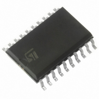
ST7FLITE39F2M6 STMicroelectronics, ST7FLITE39F2M6 Datasheet - Page 143

ST7FLITE39F2M6
Manufacturer Part Number
ST7FLITE39F2M6
Description
IC MCU 8BIT 8K FLASH 20SOIC
Manufacturer
STMicroelectronics
Series
ST7r
Datasheet
1.ST7FLITE35F2M6TR.pdf
(173 pages)
Specifications of ST7FLITE39F2M6
Core Processor
ST7
Core Size
8-Bit
Speed
16MHz
Connectivity
LINSCI, SPI
Peripherals
LVD, POR, PWM, WDT
Number Of I /o
15
Program Memory Size
8KB (8K x 8)
Program Memory Type
FLASH
Eeprom Size
256 x 8
Ram Size
384 x 8
Voltage - Supply (vcc/vdd)
2.7 V ~ 5.5 V
Data Converters
A/D 7x10b
Oscillator Type
Internal
Operating Temperature
-40°C ~ 85°C
Package / Case
20-SOIC (7.5mm Width)
Processor Series
ST7FLITE3x
Core
ST7
Data Bus Width
8 bit
Data Ram Size
384 B
Interface Type
LINSCI, SPI
Maximum Clock Frequency
8 MHz
Number Of Programmable I/os
15
Number Of Timers
4
Maximum Operating Temperature
+ 85 C
Mounting Style
SMD/SMT
Development Tools By Supplier
ST7FLITE-SK/RAIS, ST7MDT10-DVP3, ST7MDT10-EMU3, STX-RLINK
Minimum Operating Temperature
- 40 C
On-chip Adc
10 bit, 7 Channel
For Use With
497-8406 - BOARD STF20NM50FD/STF7LITE39BF2497-8403 - BOARD DEMO STCC08 AC SW DETECTOR497-6398 - BOARD EVAL ST7FLITE39/STM1403497-5858 - EVAL BOARD PLAYBACK ST7FLITE497-5514 - EVAL BOARD THERMO CONTROL REFRIG497-5049 - KIT STARTER RAISONANCE ST7FLITE
Lead Free Status / RoHS Status
Lead free / RoHS Compliant
Other names
497-5641-5
STFLITE39F2M6
STFLITE39F2M6
Available stocks
Company
Part Number
Manufacturer
Quantity
Price
13.5 CLOCK AND TIMING CHARACTERISTICS
Subject to general operating conditions for V
13.5.1 General Timings
13.5.2 External Clock Source
Notes:
1. Guaranteed by Design. Not tested in production.
2. Data based on typical application software.
3. Time measured between interrupt event and interrupt vector fetch. ∆t
ish the current instruction execution.
4. Data based on design simulation and/or technology characteristics, not tested in production.
Figure 83. Typical Application with an External Clock Source
t
t
w(OSC1H) or
V
Symbol
w(OSC1L) or
V
V
t
V
t
t
c(INST)
OSC1H
OSC1L
r(OSC1) or
f(OSC1) or
OSC1H
t
OSC1L
v(IT)
Symbol
or V
or V
or V
or V
I
L
t
t
t
t
CLKINH
Instruction cycle time
Interrupt reaction time
t
CLKINL
w(CLKINH)
w(CLKINL)
r(CLKIN)
f(CLKIN)
v(IT)
CLKIN_H
CLKIN_L
EXTERNAL
CLOCK SOURCE
= ∆t
c(INST)
Parameter
OSC1/CLKIN input pin high level voltage
OSC1/CLKIN input pin low level voltage
OSC1/CLKIN high or low time
OSC1/CLKIN rise or fall time
OSCx/CLKIN Input leakage current
+ 10
t
r(OSC1 or CLKIN)
3)
1)
Parameter
t
f(OSC1 or CLKIN)
OSC2
OSC1/CLKIN
90%
f
f
DD
CPU
CPU
10%
, f
4)
=8MHz
=8MHz
4)
OSC
Conditions
, and T
t
w(OSC1H or CLKINH)
Not connected internally
see
V
SS
A
Conditions
.
c(INST)
≤V
Figure 83
IN
≤V
I
L
is the number of t
DD
t
w(OSC1L or CLKINL)
1.25
Min
250
10
2
0.7xV
f
OSC
Min
V
15
SS
Typ
ST72XXX
375
DD
3
CPU
2)
Typ
cycles needed to fin-
ST7LITE3xF2
1500
Max
2.75
12
22
0.3xV
Max
V
±1
15
DD
DD
143/173
Unit
t
t
CPU
CPU
ns
µs
Unit
µA
ns
V


