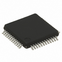
ST72F63BH2T1 STMicroelectronics, ST72F63BH2T1 Datasheet - Page 13

ST72F63BH2T1
Manufacturer Part Number
ST72F63BH2T1
Description
IC MCU 8BIT 8K FLASH 48-LQFP
Manufacturer
STMicroelectronics
Series
ST7r
Datasheet
1.ST72F63BD6U1TR.pdf
(186 pages)
Specifications of ST72F63BH2T1
Core Processor
ST7
Core Size
8-Bit
Speed
8MHz
Connectivity
I²C, SCI, USB
Peripherals
DMA, LVD, POR, PWM, WDT
Number Of I /o
27
Program Memory Size
8KB (8K x 8)
Program Memory Type
FLASH
Ram Size
384 x 8
Voltage - Supply (vcc/vdd)
4 V ~ 5.5 V
Data Converters
A/D 12x8b
Oscillator Type
External
Operating Temperature
0°C ~ 70°C
Package / Case
48-LQFP
Processor Series
ST72F6x
Core
ST7
Data Bus Width
8 bit
Data Ram Size
384 B
Interface Type
I2C, SCI
Maximum Clock Frequency
8 MHz
Number Of Programmable I/os
27
Number Of Timers
1
Maximum Operating Temperature
+ 70 C
Mounting Style
SMD/SMT
Development Tools By Supplier
ST7MDTU3-EPB/US, ST7MDTULS-EVAL, ST72F63B-SK/RAIS, ST7MDTU3-EMU3, STX-RLINK
Minimum Operating Temperature
0 C
On-chip Adc
8 bit, 8 Channel / 8 bit, 12 Channel
For Use With
497-5521 - EVAL BOARD LOW SPEED USB
Lead Free Status / RoHS Status
Lead free / RoHS Compliant
Eeprom Size
-
Lead Free Status / Rohs Status
Details
Available stocks
Company
Part Number
Manufacturer
Quantity
Price
Company:
Part Number:
ST72F63BH2T1
Manufacturer:
STMicroelectronics
Quantity:
10 000
- Current page: 13 of 186
- Download datasheet (3Mb)
ST7263Bxx
2
2.1
Note:
2.2
2.3
Note:
2.4
Note:
2.5
Note:
1
2
Pin description
RESET signal (bidirectional)
It is active low and forces the initialization of the MCU. This event is the top priority non
maskable interrupt. This pin is switched low when the Watchdog is triggered or the V
low. It can be used to reset external peripherals.
Adding two 100 nF decoupling capacitors on the Reset pin (respectively connected to V
and V
OSCIN/OSCOUT: input/output oscillator pin
These pins connect a parallel-resonant crystal, or an external source, to the on-chip
oscillator.
V
Main power supply and ground voltages
To enhance the reliability of operation, it is recommended that V
together on the application board. This also applies to V
V
Power supply and ground voltages for analog peripherals.
To enhance the reliability of operation, it is recommended that V
together on the application board. This also applies to V
Alternate functions
Several pins of the I/O ports assume software programmable alternate functions as shown
in the pin description.
The USBOE alternate function is mapped on Port C2 in 32/34/48 pin devices. In SO24
devices it is mapped on Port B1.
The timer OCMP1 alternate function is mapped on Port A6 in 32/34/48 pin devices. In SO24
devices it is not available.
DD
DDA
/V
SS
/V
) will significantly improve product electromagnetic susceptibility performance.
SS
SSA
Doc ID 7516 Rev 8
SSA
SSA
and V
and V
DDA
DDA
SS
SS
and V
and V
.
.
DD
DD
Pin description
be connected
be connected
DD
13/186
DD
is
Related parts for ST72F63BH2T1
Image
Part Number
Description
Manufacturer
Datasheet
Request
R

Part Number:
Description:
KIT STARTER LOW COST ST7
Manufacturer:
STMicroelectronics
Datasheet:

Part Number:
Description:
LOW SPEED USB 8-BIT MCU FAMILY WITH FLASH/ROM, UP TO 512 BYTES RAM, 8-BIT ADC, WDG, TIMER, SCI & I�C
Manufacturer:
STMICROELECTRONICS [STMicroelectronics]
Datasheet:

Part Number:
Description:
STMicroelectronics [RIPPLE-CARRY BINARY COUNTER/DIVIDERS]
Manufacturer:
STMicroelectronics
Datasheet:

Part Number:
Description:
STMicroelectronics [LIQUID-CRYSTAL DISPLAY DRIVERS]
Manufacturer:
STMicroelectronics
Datasheet:

Part Number:
Description:
BOARD EVAL FOR MEMS SENSORS
Manufacturer:
STMicroelectronics
Datasheet:

Part Number:
Description:
NPN TRANSISTOR POWER MODULE
Manufacturer:
STMicroelectronics
Datasheet:

Part Number:
Description:
TURBOSWITCH ULTRA-FAST HIGH VOLTAGE DIODE
Manufacturer:
STMicroelectronics
Datasheet:

Part Number:
Description:
Manufacturer:
STMicroelectronics
Datasheet:

Part Number:
Description:
DIODE / SCR MODULE
Manufacturer:
STMicroelectronics
Datasheet:

Part Number:
Description:
DIODE / SCR MODULE
Manufacturer:
STMicroelectronics
Datasheet:

Part Number:
Description:
Search -----> STE16N100
Manufacturer:
STMicroelectronics
Datasheet:

Part Number:
Description:
Search ---> STE53NA50
Manufacturer:
STMicroelectronics
Datasheet:


