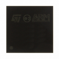
STR912FAZ44H6 STMicroelectronics, STR912FAZ44H6 Datasheet - Page 12

STR912FAZ44H6
Manufacturer Part Number
STR912FAZ44H6
Description
MCU 512KB FLASH 96K RAM 144LFBGA
Manufacturer
STMicroelectronics
Series
STR9r
Datasheet
1.STEVAL-IFW001V1.pdf
(102 pages)
Specifications of STR912FAZ44H6
Core Processor
ARM9
Core Size
32-Bit
Speed
96MHz
Connectivity
CAN, EBI/EMI, Ethernet, I²C, IrDA, Microwire, SPI, SSI, SSP, UART/USART, USB
Peripherals
Brown-out Detect/Reset, DMA, Motor Control PWM, POR, PWM, WDT
Number Of I /o
80
Program Memory Size
512KB (512K x 8)
Program Memory Type
FLASH
Ram Size
96K x 8
Voltage - Supply (vcc/vdd)
1.65 V ~ 2 V
Data Converters
A/D 8x10b
Oscillator Type
Internal
Operating Temperature
-40°C ~ 85°C
Package / Case
144-LFBGA
Processor Series
STR912x
Core
ARM966E-S
Data Bus Width
16 bit, 32 bit
Data Ram Size
96 KB
Interface Type
CAN, I2C, IrDA, SSP, UART, USB
Maximum Clock Frequency
96 MHz
Number Of Programmable I/os
80
Number Of Timers
4
Maximum Operating Temperature
+ 85 C
Mounting Style
SMD/SMT
3rd Party Development Tools
EWARM, EWARM-BL, MCBSTR9, MCBSTR9U, MCBSTR9UME, KSDK-STR912-PLUS, MDK-ARM, RL-ARM, ULINK2
Development Tools By Supplier
STR9-COMSTICK, STR910-EVAL, STR91X-SK/HIT, STR91X-SK/IAR, STR91X-SK/KEI, STR91X-SK/RAI, STR9-DK/RAIS, STR91X-DK/IAR, STX-PRO/RAIS, STR912-D/RAIS, STR79-RVDK/CPP, STR79-RVDKCPP/9, STR79-RVDK, STR79-RVDK/9, STR9-RVDK/BAS, STR79-RVDK/UPG
Minimum Operating Temperature
- 40 C
On-chip Adc
10 bit, 8 Channel
For Use With
497-8267 - BOARD EVAL BASED ON STR9497-8262 - BOARD EVAL BASED ON STR912FAMCBSTR9UME - BOARD EVAL MCBSTR9 + ULINK-MEMCBSTR9U - BOARD EVAL MCBSTR9 + ULINK2MCBSTR9 - BOARD EVAL STM STR9 SERIES497-5067 - BOARD EVAL FOR STR910 FAMILY497-5066 - KIT STARTER KEIL FOR STR910497-5065 - KIT STARTER IAR KICKSTART STR912497-5064 - KIT STARTER FOR STR910 FAMILY497-5046 - KIT TOOL FOR ST7/UPSD/STR7 MCU
Lead Free Status / RoHS Status
Lead free / RoHS Compliant
Eeprom Size
-
Lead Free Status / Rohs Status
Details
Other names
497-6286
Available stocks
Company
Part Number
Manufacturer
Quantity
Price
Company:
Part Number:
STR912FAZ44H6
Manufacturer:
STM
Quantity:
3 000
Company:
Part Number:
STR912FAZ44H6
Manufacturer:
STMicroelectronics
Quantity:
10 000
Part Number:
STR912FAZ44H6
Manufacturer:
ST
Quantity:
20 000
Company:
Part Number:
STR912FAZ44H6T
Manufacturer:
STMicroelectronics
Quantity:
10 000
Functional overview
3
3.1
3.2
3.3
3.4
3.4.1
12/102
Functional overview
System-in-a-package (SiP)
The STR91xFA is a SiP device, comprised of two stacked die. One die is the ARM966E-S
CPU with peripheral interfaces and analog functions, and the other die is the burst Flash.
The two die are connected to each other by a custom high-speed 32-bit burst memory
interface and a serial JTAG test/programming interface.
Package choice
STR91xFA devices are available in 128-pin (14 x 14 mm) and 80-pin (12 x 12 mm) LQFP
and LFBGA144 (10 x 10 mm) packages. Refer to
list of available peripherals for each of the package choices.
ARM966E-S CPU core
The ARM966E-S core inherently has separate instruction and data memory interfaces
(Harvard architecture), allowing the CPU to simultaneously fetch an instruction, and read or
write a data item through two Tightly-Coupled Memory (TCM) interfaces as shown in
Figure
reduction in cycle count per instruction. In addition to this, a 5-stage pipeline is used to
increase the amount of operational parallelism, giving the most performance out of each
clock cycle.
Ten DSP-enhanced instruction extensions are supported by this core, including single-cycle
execution of 32x16 Multiply-Accumulate, saturating addition/subtraction, and count leading-
zeros.
The ARM966E-S core is binary compatible with 32-bit ARM7 code and 16-bit Thumb
Burst Flash memory interface
A burst Flash memory interface
(I-TCM) path of the ARM966E-S core. Also in this path is an 8-instruction Pre-Fetch Queue
(PFQ) and a 15-entry Branch Cache (BC), enabling the ARM966E-S core to perform up to
96 MIPS while executing code directly from Flash memory. This architecture provides high
performance levels without a costly instruction SRAM, instruction cache, or external
SDRAM. Eliminating the instruction cache also means interrupt latency is reduced and code
execution becomes more deterministic.
Pre-fetch queue (PFQ)
As the CPU core accesses sequential instructions through the I-TCM, the PFQ always looks
ahead and will pre-fetch instructions, taking advantage any idle bus cycles due to variable
length instructions. The PFQ will fetch 32-bits at a time from the burst Flash memory at a
rate of up to 96 MHz.
1. The result is streamlined CPU Load and Store operations and a significant
Doc ID 13495 Rev 6
(Figure
1) has been integrated into the Instruction TCM
Table 2: Device summary on page 11
STR91xFAxxx
®
code.
for a


