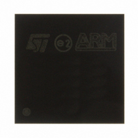
STR912FAZ44H6 STMicroelectronics, STR912FAZ44H6 Datasheet - Page 38

STR912FAZ44H6
Manufacturer Part Number
STR912FAZ44H6
Description
MCU 512KB FLASH 96K RAM 144LFBGA
Manufacturer
STMicroelectronics
Series
STR9r
Datasheet
1.STEVAL-IFW001V1.pdf
(102 pages)
Specifications of STR912FAZ44H6
Core Processor
ARM9
Core Size
32-Bit
Speed
96MHz
Connectivity
CAN, EBI/EMI, Ethernet, I²C, IrDA, Microwire, SPI, SSI, SSP, UART/USART, USB
Peripherals
Brown-out Detect/Reset, DMA, Motor Control PWM, POR, PWM, WDT
Number Of I /o
80
Program Memory Size
512KB (512K x 8)
Program Memory Type
FLASH
Ram Size
96K x 8
Voltage - Supply (vcc/vdd)
1.65 V ~ 2 V
Data Converters
A/D 8x10b
Oscillator Type
Internal
Operating Temperature
-40°C ~ 85°C
Package / Case
144-LFBGA
Processor Series
STR912x
Core
ARM966E-S
Data Bus Width
16 bit, 32 bit
Data Ram Size
96 KB
Interface Type
CAN, I2C, IrDA, SSP, UART, USB
Maximum Clock Frequency
96 MHz
Number Of Programmable I/os
80
Number Of Timers
4
Maximum Operating Temperature
+ 85 C
Mounting Style
SMD/SMT
3rd Party Development Tools
EWARM, EWARM-BL, MCBSTR9, MCBSTR9U, MCBSTR9UME, KSDK-STR912-PLUS, MDK-ARM, RL-ARM, ULINK2
Development Tools By Supplier
STR9-COMSTICK, STR910-EVAL, STR91X-SK/HIT, STR91X-SK/IAR, STR91X-SK/KEI, STR91X-SK/RAI, STR9-DK/RAIS, STR91X-DK/IAR, STX-PRO/RAIS, STR912-D/RAIS, STR79-RVDK/CPP, STR79-RVDKCPP/9, STR79-RVDK, STR79-RVDK/9, STR9-RVDK/BAS, STR79-RVDK/UPG
Minimum Operating Temperature
- 40 C
On-chip Adc
10 bit, 8 Channel
For Use With
497-8267 - BOARD EVAL BASED ON STR9497-8262 - BOARD EVAL BASED ON STR912FAMCBSTR9UME - BOARD EVAL MCBSTR9 + ULINK-MEMCBSTR9U - BOARD EVAL MCBSTR9 + ULINK2MCBSTR9 - BOARD EVAL STM STR9 SERIES497-5067 - BOARD EVAL FOR STR910 FAMILY497-5066 - KIT STARTER KEIL FOR STR910497-5065 - KIT STARTER IAR KICKSTART STR912497-5064 - KIT STARTER FOR STR910 FAMILY497-5046 - KIT TOOL FOR ST7/UPSD/STR7 MCU
Lead Free Status / RoHS Status
Lead free / RoHS Compliant
Eeprom Size
-
Lead Free Status / Rohs Status
Details
Other names
497-6286
Available stocks
Company
Part Number
Manufacturer
Quantity
Price
Company:
Part Number:
STR912FAZ44H6
Manufacturer:
STM
Quantity:
3 000
Company:
Part Number:
STR912FAZ44H6
Manufacturer:
STMicroelectronics
Quantity:
10 000
Part Number:
STR912FAZ44H6
Manufacturer:
ST
Quantity:
20 000
Company:
Part Number:
STR912FAZ44H6T
Manufacturer:
STMicroelectronics
Quantity:
10 000
Functional overview
3.27
38/102
External memory interface (EMI)
STR91xFA devices in 128-pin and 144-ball packages offer an external memory bus for
connecting external parallel peripherals and memories. The EMI bus resides on ports 7, 8,
and 9 and operates with either an 8 or 16-bit data path. The configuration of 8 or 16 bit
mode is specified by CPU firmware writing to configuration registers at run-time. If the
application does not use the EMI bus, then these port pins may be used for general purpose
I/O as shown in
The EMI has the following features:
●
●
●
●
●
To use all 24 address bits, the following applies: 8 bits of lowest-order data and 8 bits of
lowest-order address are multiplexed on port 8. On port 9, 8-bits of mid-order address are
multiplexed with 8 bits of data, but these 8 data values are always at logic zero on this port
during a write operation, and these 8 data bits are ignored during a read operation. An
external latch device is needed to de-multiplex the mid-order 8 address bits that are
generated on port 8. Port 7 outputs the 8 highest-order address signals directly (not
multiplexed). The output signal on pin EMI_ALE is used to demultiplex the signals on ports 8
and 9, and the polarity of EMI_ALE is programmable. The output signal on pin
Supports static asynchronous memory access cycles, including page mode for non-
mux operation. The bus control signals include:
–
–
–
–
Four configurable memory regions, each with a chip select output (EMI_CS0n ...
EMI_CS3n)
Programmable wait states per memory region for both write and read operations
16-bit multiplexed data mode
address are multiplexed together on ports 8 and 9, while port 7 contains eight more
high-order address signals. The output signal on pin EMI_ALE is used to demultiplex
the signals on ports 8 and 9, and the polarity of EMI_ALE is programmable. The output
signals on pins EMI_BWR_WRLn and EMI_WRHn are the write strobes for the low and
high data bytes respectively. The output signal EMI_RDn is the read strobe for both the
low and high data bytes.
8-bit multiplexed data mode: This is a variant of the 16-bit multiplexed mode.
Although this mode can provide 24 bits of address and 8 bits of data, it does require an
external latch device on Port 8. However, this mode is most efficient when connecting
devices that only require 8 bits of address on an 8-bit multiplexed address/data bus,
and have simple read, write, and latch inputs as shown in
EMI_RDn - read signal, x8 or x16 mode
EMI_BWR_WRLn - write signal in x8 mode and write low byte signal in x16 mode
EMI_WRHn - write high byte signal in x16 mode
EMI_ALE - address latch signal for x8 or x16 mux bus mode with programmable
polarity
Table
8.
Doc ID 13495 Rev 6
(Figure
4): 16 bits of data and 16 bits of low-order
Figure 5
STR91xFAxxx


