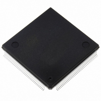
ST10F269Z2Q6 STMicroelectronics, ST10F269Z2Q6 Datasheet - Page 21

ST10F269Z2Q6
Manufacturer Part Number
ST10F269Z2Q6
Description
MCU 16BIT 256K FLASH 144PQFP
Manufacturer
STMicroelectronics
Series
ST10r
Specifications of ST10F269Z2Q6
Core Processor
ST10
Core Size
16-Bit
Speed
40MHz
Connectivity
CAN, EBI/EMI, SSC, UART/USART
Peripherals
POR, PWM, WDT
Number Of I /o
111
Program Memory Size
256KB (256K x 8)
Program Memory Type
FLASH
Ram Size
12K x 8
Voltage - Supply (vcc/vdd)
4.5 V ~ 5.5 V
Data Converters
A/D 16x10b
Oscillator Type
Internal
Operating Temperature
-40°C ~ 85°C
Package / Case
144-QFP
Controller Family/series
ST10
No. Of I/o's
111
Ram Memory Size
12KB
Cpu Speed
40MHz
No. Of Timers
5
Embedded Interface Type
CAN, SSC, USART
Rohs Compliant
Yes
Processor Series
ST10F26x
Core
ST10
Data Bus Width
16 bit
Data Ram Size
12 KB
Interface Type
CAN, SSC, USART
Maximum Clock Frequency
40 MHz
Number Of Programmable I/os
111
Number Of Timers
2 x 16 bit
Operating Supply Voltage
0.3 V to 4 V
Maximum Operating Temperature
+ 85 C
Mounting Style
SMD/SMT
Minimum Operating Temperature
- 40 C
On-chip Adc
16 bit x 10 bit
Lead Free Status / RoHS Status
Lead free / RoHS Compliant
Eeprom Size
-
Lead Free Status / Rohs Status
Details
Other names
497-4833
Available stocks
Company
Part Number
Manufacturer
Quantity
Price
Company:
Part Number:
ST10F269Z2Q6
Manufacturer:
ST
Quantity:
201
Company:
Part Number:
ST10F269Z2Q6
Manufacturer:
ST
Quantity:
745
Company:
Part Number:
ST10F269Z2Q6
Manufacturer:
STMicroelectronics
Quantity:
10 000
Part Number:
ST10F269Z2Q6
Manufacturer:
ST
Quantity:
20 000
ST10F269
5.3.5 - Flash Protection Register
The Flash Protection register is a non-volatile register that contains the protection status. This register
can be read by using the Read Protection Status (RP) command, and programmed by using the dedi-
cated Set Protection command.
Flash Protection Register (PR)
*Not avalaible for 128K versions (reserved areas)
5.3.6 - Instructions Description
Twelve instructions dedicated to Flash memory
accesses are defined as follow:
Read/Reset (RD). The Read/Reset instruction
consist of one write cycle with data XXF0h. it can
be optionally preceded by two CI enable coded
cycles (data xxA8h at address 1554h + data
xx54h at address 2AA8h). Any successive read
cycle following a Read/Reset instruction will read
the memory array. A Wait cycle of 10µs is
necessary after a Read/Reset command if the
memory was in program or Erase mode.
Program Word (PW). This instruction uses four
write cycles. After the two Cl enable coded cycles,
the Program Word command xxA0h is written at
address 1554h. The following write cycle will latch
the address and data of the word to be
programmed. Memory programming can be done
only by writing 0's instead of 1's, otherwise an
error occurs. During programming, the Flash
BPx
CP
CP
15
14
-
13
-
12
-
Block x Protection Bit (x = 0...6)
‘0’: the Block Protection is enabled for block x. Programming or erasing the block is not
possible, unless a Block Temporary Unprotection command is issued.
1’: the Block Protection is disabled for block x.
Bit is ‘1’ by default, and can be programmed permanently to ‘0’ using the Set Protection
command but then cannot be set to ‘1’ again. It is therefore possible to temporally disable the
Block Protection using the Block Temporary Unprotection instruction.
Code Protection Bit
‘0’: the Flash Code Protection is enabled. Read accesses to the Flash for execution not
performed in the Flash itself are not allowed, the returned value will be 009Bh, whatever the
content of the Flash is.
1’: the Flash Code Protection is disabled: read accesses to the Flash from external or internal
RAM are allowed
Bit is ‘1’ by default, and can be programmed permanently to ‘0’ using the Set Protection
command but then cannot be set to ‘1’ again. It is therefore possible to temporally disable the
Code Protection using the Code Temporary Unprotection instruction.
11
-
10
-
9
-
8
-
7
-
Status is checked by reading the Flash Status bit
FSB.2, FSB.5, FSB.6 and FSB.7 which show the
status of the EPC. FSB.2, FSB.6 and FSB.7
determine if programming is on going or has
completed, and FSB.5 allows a check to be made
for any possible error.
Block Erase (BE). This instruction uses a
minimum of six command cycles. The erase
enable command xx80h is written at address
1554h after the two-cycle CI enable sequence.
The erase confirm code xx30h must be written at
an address related to the block to be erased
preceded by the execution of a second CI enable
sequence. Additional erase confirm codes must
be given to erase more than one block in parallel.
Additional erase confirm commands must be
written within a defined time-out period. The input
of a new Block Erase command will restart the
time-out period.
When this time-out period has elapsed, the erase
starts. The status of the internal timer can be
monitored through the level of FSB.3, if FSB.3 is
‘0’, the Block Erase command has been given and
BP6* BP5*
6
5 - INTERNAL FLASH MEMORY
5
BP4
4
BP3
3
BP2
2
BP1
1
21/184
BP0
0


