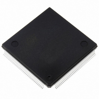
ST10F269Z2Q6 STMicroelectronics, ST10F269Z2Q6 Datasheet - Page 68

ST10F269Z2Q6
Manufacturer Part Number
ST10F269Z2Q6
Description
MCU 16BIT 256K FLASH 144PQFP
Manufacturer
STMicroelectronics
Series
ST10r
Specifications of ST10F269Z2Q6
Core Processor
ST10
Core Size
16-Bit
Speed
40MHz
Connectivity
CAN, EBI/EMI, SSC, UART/USART
Peripherals
POR, PWM, WDT
Number Of I /o
111
Program Memory Size
256KB (256K x 8)
Program Memory Type
FLASH
Ram Size
12K x 8
Voltage - Supply (vcc/vdd)
4.5 V ~ 5.5 V
Data Converters
A/D 16x10b
Oscillator Type
Internal
Operating Temperature
-40°C ~ 85°C
Package / Case
144-QFP
Controller Family/series
ST10
No. Of I/o's
111
Ram Memory Size
12KB
Cpu Speed
40MHz
No. Of Timers
5
Embedded Interface Type
CAN, SSC, USART
Rohs Compliant
Yes
Processor Series
ST10F26x
Core
ST10
Data Bus Width
16 bit
Data Ram Size
12 KB
Interface Type
CAN, SSC, USART
Maximum Clock Frequency
40 MHz
Number Of Programmable I/os
111
Number Of Timers
2 x 16 bit
Operating Supply Voltage
0.3 V to 4 V
Maximum Operating Temperature
+ 85 C
Mounting Style
SMD/SMT
Minimum Operating Temperature
- 40 C
On-chip Adc
16 bit x 10 bit
Lead Free Status / RoHS Status
Lead free / RoHS Compliant
Eeprom Size
-
Lead Free Status / Rohs Status
Details
Other names
497-4833
Available stocks
Company
Part Number
Manufacturer
Quantity
Price
Company:
Part Number:
ST10F269Z2Q6
Manufacturer:
ST
Quantity:
201
Company:
Part Number:
ST10F269Z2Q6
Manufacturer:
ST
Quantity:
745
Company:
Part Number:
ST10F269Z2Q6
Manufacturer:
STMicroelectronics
Quantity:
10 000
Part Number:
ST10F269Z2Q6
Manufacturer:
ST
Quantity:
20 000
12 - PARALLEL PORTS
12.5 - Port 2
If this 16-bit port is used for general purpose I/O, the direction of each line can be configured via the
corresponding direction register DP2. Each port line can be switched into push/pull or open drain mode
via the open drain control register ODP2.
P2 (FFC0h / E0h)
DP2 (FFC2h / E1h)
ODP2 (F1C2h / E1h)
12.5.1 - Alternate Functions of Port 2
All Port 2 lines (P2.15...P2.0) serve as capture
inputs or compare outputs (CC15IO...CC0IO) for
the CAPCOM1 unit.
When a Port 2 line is used as a capture input, the
state of the input latch, which represents the state
of the port pin, is directed to the CAPCOM unit via
the line “Alternate Pin Data Input”. If an external
capture trigger signal is used, the direction of the
respective pin must be set to input.
If the direction is set to output, the state of the port
output latch will be read since the pin represents
the state of the output latch.
This can be used to trigger a capture event
through software by setting or clearing the port
latch. Note that in the output configuration, no
68/184
ODP2
P2.15 P2.14 P2.13 P2.12 P2.11 P2.10 P2.9
P2.y
DP2.y
ODP2.y
DP2
RW
RW
RW
.15
.15
15
15
15
ODP2
DP2
RW
RW
RW
.14
.14
14
14
14
ODP2
DP2
RW
RW
RW
.13
.13
13
13
13
Port Data Register P2 Bit y
Port Direction Register DP2 Bit y
DP2.y = 0: Port line P2.y is an input (high-impedance)
DP2.y = 1: Port line P2.y is an output
Port 2 Open Drain Control Register Bit y
ODP2.y = 0: Port line P2.y output driver in push/pull mode
ODP2.y = 1: Port line P2.y output driver in open drain mode
ODP2
DP2
RW
RW
RW
.12
.12
12
12
12
ODP2
DP2
RW
RW
RW
.11
.11
11
11
11
ODP2
DP2
RW
RW
RW
.10
.10
10
10
10
ODP2
DP2
RW
RW
RW
.9
.9
9
9
9
ODP2
P2.8
DP2
RW
RW
RW
.8
.8
8
8
8
ESFR
SFR
SFR
ODP2
P2.7
DP2
RW
RW
RW
external device may drive the pin, otherwise
conflicts would occur.
When a Port 2 line is used as a compare output
(compare modes 1 and 3), the compare event (or
the timer overflow in compare mode 3) directly
effects the port output latch. In compare mode 1,
when a valid compare match occurs, the state of
the port output latch is read by the CAPCOM
control hardware via the line “Alternate Latch Data
Input”, inverted, and written back to the latch via
the line “Alternate Data Output”.
The port output latch is clocked by the signal
“Compare Trigger” which is generated by the
CAPCOM unit. In compare mode 3, when a match
occurs, the value '1' is written to the port output
latch via the line “Alternate Data Output”. When
an overflow of the corresponding timer occurs, a
'0' is written to the port output latch. In both cases,
.7
.7
7
7
7
ODP2
P2.6
DP2
RW
RW
RW
.6
.6
6
6
6
ODP2
P2.5
DP2
RW
RW
RW
.5
.5
5
5
5
ODP2
P2.4
DP2
RW
RW
RW
.4
.4
4
4
4
ODP2
P2.3
DP2
RW
RW
RW
.3
.3
3
3
3
Reset Value: 0000h
Reset Value: 0000h
Reset Value: 0000h
ODP2
P2.2
DP2
RW
RW
RW
.2
.2
2
2
2
ODP2
ST10F269
P2.1
DP2
RW
RW
RW
.1
.1
1
1
1
ODP2
P2.0
DP2
RW
RW
RW
.0
.0
0
0
0


