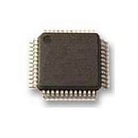
MC9S08MP16VLF Freescale Semiconductor, MC9S08MP16VLF Datasheet - Page 30

MC9S08MP16VLF
Manufacturer Part Number
MC9S08MP16VLF
Description
MCU 8BIT .25U SGF FLASH 48-LQFP
Manufacturer
Freescale Semiconductor
Series
HCS08r
Datasheet
1.MC9S08MP12VWL.pdf
(36 pages)
Specifications of MC9S08MP16VLF
Core Processor
HCS08
Core Size
8-Bit
Speed
51.34MHz
Connectivity
I²C, LIN, SCI, SPI
Peripherals
LVD, POR, PWM, WDT
Number Of I /o
40
Program Memory Size
16KB (16K x 8)
Program Memory Type
FLASH
Ram Size
1K x 8
Voltage - Supply (vcc/vdd)
2.7 V ~ 5.5 V
Data Converters
A/D 13x12b, D/A 3x5b
Oscillator Type
Internal
Operating Temperature
-40°C ~ 105°C
Package / Case
48-LQFP
Processor Series
S08MP
Core
HCS08
Data Bus Width
8 bit
Data Ram Size
1 KB
Interface Type
SCI
Maximum Clock Frequency
51.34 MHz
Number Of Programmable I/os
40
Number Of Timers
2
Operating Supply Voltage
- 0.3 V to + 5.8 V
Maximum Operating Temperature
+ 105 C
Mounting Style
SMD/SMT
3rd Party Development Tools
EWS08
Development Tools By Supplier
DEMO9S08MP16
Minimum Operating Temperature
- 40 C
On-chip Adc
12 bit, 13 Channel
On-chip Dac
3 DAC, 5 bit
Lead Free Status / RoHS Status
Lead free / RoHS Compliant
Eeprom Size
-
Lead Free Status / Rohs Status
Lead free / RoHS Compliant
Available stocks
Company
Part Number
Manufacturer
Quantity
Price
Company:
Part Number:
MC9S08MP16VLF
Manufacturer:
Freescale Semiconductor
Quantity:
10 000
Electrical Characteristics
2.14.4
Table 19
30
1
2
3
4
5
6
and
Num
Refer to
All timing is shown with respect to 20% V
timing assumes slew rate control disabled and high drive strength enabled for SPI output pins.
Time to data active from high-impedance state.
Hold time to high-impedance state.
Maximum baud rate must be limited to 8 MHz.
Maximum baud rate must be limited to 5 MHz due to input filter characteristics.
10
11
12
1
2
3
4
5
6
7
8
9
Figure 22
SPI
1
Figure 22
C
D
D
D
D
D
D
D
D
D
D
D
D
through
Cycle time
Enable lead time
Enable lag time
Clock (SPSCK) high time
Master and Slave
Clock (SPSCK) low time
Master and Slave
Data setup time (inputs)
Data hold time (inputs)
Access time, slave
Disable time, slave
Data setup time (outputs)
Data hold time (outputs)
Operating frequency
through
Figure 25
Figure
Table 19. SPI Electrical Characteristics
MC9S08MP16 Series Data Sheet, Rev. 1
describe the timing requirements for the SPI system.
Rating
3
4
25.
Master (SPIFE=0)
Master (SPIFE=1)
2
Slave (SPIFE=0)
Slave (SPIFE=1)
DD
and 70% V
Master
Master
Master
Master
Master
Master
Master
Slave
Slave
Slave
Slave
Slave
Slave
Slave
DD
, unless noted; 100 pF load on all SPI pins. All
Symbol
t
t
t
t
t
t
t
t
SCKH
t
t
SCKL
t
t
SI(M)
HI(M)
Lead
Lead
SI(S)
HI(S)
t
t
t
t
t
SCK
SCK
f
Lag
Lag
HO
HO
t
SO
SO
dis
op
A
1/2 t
1/2 t
f
f
Bus
Bus
SCK
SCK
Min
–10
–10
1/2
1/2
30
30
30
30
dc
dc
—
—
—
—
—
/4096
/4096
2
4
0
– 25
– 25
f
4096
Bus
Max
1/2
1/2
—
40
40
25
25
8
5
5
—
—
—
—
—
—
—
—
—
—
Freescale Semiconductor
5
6
6
/4
t
t
t
t
MHz
MHz
MHz
Unit
t
t
SCK
SCK
SCK
SCK
ns
ns
ns
ns
ns
ns
ns
ns
ns
ns
ns
ns
cyc
cyc


