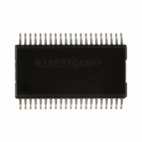
M38503G4AFP#U1 Renesas Electronics America, M38503G4AFP#U1 Datasheet - Page 29

M38503G4AFP#U1
Manufacturer Part Number
M38503G4AFP#U1
Description
IC 740/3850 MCU QZ-ROM 42SSOP
Manufacturer
Renesas Electronics America
Series
740/38000r
Datasheet
1.M38507F8AFPU1.pdf
(61 pages)
Specifications of M38503G4AFP#U1
Core Processor
740
Core Size
8-Bit
Speed
12.5MHz
Connectivity
SIO, UART/USART
Peripherals
PWM, WDT
Number Of I /o
32
Program Memory Size
16KB (16K x 8)
Program Memory Type
QzROM
Ram Size
512 x 8
Voltage - Supply (vcc/vdd)
1.8 V ~ 5.5 V
Data Converters
A/D 9x10b
Oscillator Type
Internal
Operating Temperature
-20°C ~ 85°C
Package / Case
42-SSOP
Lead Free Status / RoHS Status
Lead free / RoHS Compliant
Eeprom Size
-
Available stocks
Company
Part Number
Manufacturer
Quantity
Price
3850 Group (Spec.A QzROM version)
Rev.2.13
REJ03B0125-0213
Fig 24. Structure of serial I/O1 control registers
<Notes on serial interface>
When setting the transmit enable bit to “1”, the serial I/O1
transmit interrupt request bit is automatically set to “1”. When
not requiring the interrupt occurrence synchronized with the
transmission enabled, take the following sequence.
(1) Set the serial I/O1 transmit interrupt enable bit to “0”
(2) Set the transmit enable bit to “1”.
(3) Set the serial I/O1 transmit interrupt request bit to “0” after
(4) Set the serial I/O1 transmit interrupt enable bit to “1”
b7
b7
(disabled).
1 or more instructions have been executed.
(enabled).
Apr 17, 2009
b0
b0
UART control register
(UARTCON : address 001B
Serial I/O1 status register
(SIOSTS : address 0019
Transmit buffer empty flag (TBE)
Receive buffer full flag (RBF)
Transmit shift completion flag (TSC)
Overrun error flag (OE)
Parity error flag (PE)
Framing error flag (FE)
Summing error flag (SE)
Not used (returns “1” when read)
Character length selection bit (CHAS)
Parity enable bit (PARE)
Parity selection bit (PARS)
Stop bit length selection bit (STPS)
P2
Not used (return “1” when read)
0: Buffer full
1: Buffer empty
0: Buffer empty
1: Buffer full
0: Transmit shift in progress
1: Transmit shift completed
0: No error
1: Overrun error
0: No error
1: Parity error
0: No error
1: Framing error
0: (OE) U (PE) U (FE)=0
1: (OE) U (PE) U (FE)=1
0: 8 bits
1: 7 bits
0: Parity checking disabled
1: Parity checking enabled
0: Even parity
1: Odd parity
0: 1 stop bit
1: 2 stop bits
0: CMOS output (in output mode)
1: N-channel open drain output (in output mode)
5
/T
X
D P-channel output disable bit (POFF)
Page 27 of 56
16
)
16
)
b7
b0
Serial I/O1 control register
(SIOCON : address 001A
BRG count source selection bit (CSS)
Serial I/O1 synchronous clock selection bit (SCS)
S
Transmit interrupt source selection bit (TIC)
Transmit enable bit (TE)
Receive enable bit (RE)
Serial I/O1 mode selection bit (SIOM)
Serial I/O1 enable bit (SIOE)
0: f(X
1: f(X
0: BRG output divided by 4 when clock synchronous
1: External clock input when clock synchronous serial
0: P2
1: P2
0: Interrupt when transmit buffer has emptied
1: Interrupt when transmit shift operation is completed
0: Transmit disabled
1: Transmit enabled
0: Receive disabled
1: Receive enabled
0: Clock asynchronous (UART) serial I/O
1: Clock synchronous serial I/O
0: Serial I/O1 disabled
1: Serial I/O1 enabled
RDY1
serial I/O1 is selected, BRG output divided by 16
when UART is selected.
I/O1 is selected, external clock input divided by 16
when UART is selected.
(pins P2
(pins P2
7
7
IN
IN
output enable bit (SRDY)
pin operates as ordinary I/O pin
pin operates as S
)
)/4
4
4
to P2
to P2
7
7
operate as ordinary I/O pins)
operate as serial I/O1 pins)
16
)
RDY1
output pin


