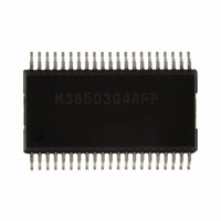
M38503G4AFP#U1 Renesas Electronics America, M38503G4AFP#U1 Datasheet - Page 33

M38503G4AFP#U1
Manufacturer Part Number
M38503G4AFP#U1
Description
IC 740/3850 MCU QZ-ROM 42SSOP
Manufacturer
Renesas Electronics America
Series
740/38000r
Datasheet
1.M38507F8AFPU1.pdf
(61 pages)
Specifications of M38503G4AFP#U1
Core Processor
740
Core Size
8-Bit
Speed
12.5MHz
Connectivity
SIO, UART/USART
Peripherals
PWM, WDT
Number Of I /o
32
Program Memory Size
16KB (16K x 8)
Program Memory Type
QzROM
Ram Size
512 x 8
Voltage - Supply (vcc/vdd)
1.8 V ~ 5.5 V
Data Converters
A/D 9x10b
Oscillator Type
Internal
Operating Temperature
-20°C ~ 85°C
Package / Case
42-SSOP
Lead Free Status / RoHS Status
Lead free / RoHS Compliant
Eeprom Size
-
Available stocks
Company
Part Number
Manufacturer
Quantity
Price
3850 Group (Spec.A QzROM version)
Rev.2.13
REJ03B0125-0213
PWM (PWM: Pulse Width Modulation)
The 3850 group (spec.A) has a PWM function with an 8-bit
resolution, based on a signal that is the clock input X
clock input divided by 2.
• Data Setting
The PWM output pin also functions as port P4
period by the PWM prescaler, and set the “H” term of output
pulse by the PWM register.
If the value in the PWM prescaler is n and the value in the PWM
register is m (where n = 0 to 255 and m = 0 to 255):
PWM period = 255 × (n+1) / f(X
Output pulse “H” term = PWM period × m / 255
Fig 30. Block diagram of PWM function
(X
CIN
= 31.875 × (n+1) µs
= 0.125 × (n+1) × m µs
(when f(X
(when f(X
at low-speed mode)
Apr 17, 2009
IN
IN
) = 8 MHz, count source selection bit = “0”)
) = 8 MHz, count source selection bit = “0”)
X
IN
Data bus
1/2
IN
Page 31 of 56
)
“0”
Count source
selection bit
“1”
4
. Set the PWM
prescaler pre-latch
PWM prescaler
prescaler latch
IN
PWM
PWM
or that
Transfer control circuit
• PWM Operation
When bit 0 (PWM enable bit) of the PWM control register is set
to “1”, operation starts by initializing the PWM output circuit,
and pulses are output starting at an “H”.
If the PWM register or PWM prescaler is updated during PWM
output, the pulses will change in the cycle after the one in which
the change was made.
Fig 29. Timing of PWM period
register pre-latch
PWM output
register latch
PWM register
PWM
m : Contents of PWM register
n : Contents of PWM prescaler
T : PWM period (when f(X
PWM
selection bit = “0”)
31.875 × m × (n+1)
T = [31.875 × (n+1)] µs
Port P4
255
PWM function enable bit
4
IN
latch
) = 8 MHz, count source
µs
Port P4
4


