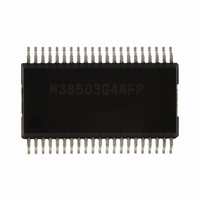
M38503G4AFP#U1 Renesas Electronics America, M38503G4AFP#U1 Datasheet - Page 30

M38503G4AFP#U1
Manufacturer Part Number
M38503G4AFP#U1
Description
IC 740/3850 MCU QZ-ROM 42SSOP
Manufacturer
Renesas Electronics America
Series
740/38000r
Datasheet
1.M38507F8AFPU1.pdf
(61 pages)
Specifications of M38503G4AFP#U1
Core Processor
740
Core Size
8-Bit
Speed
12.5MHz
Connectivity
SIO, UART/USART
Peripherals
PWM, WDT
Number Of I /o
32
Program Memory Size
16KB (16K x 8)
Program Memory Type
QzROM
Ram Size
512 x 8
Voltage - Supply (vcc/vdd)
1.8 V ~ 5.5 V
Data Converters
A/D 9x10b
Oscillator Type
Internal
Operating Temperature
-20°C ~ 85°C
Package / Case
42-SSOP
Lead Free Status / RoHS Status
Lead free / RoHS Compliant
Eeprom Size
-
Available stocks
Company
Part Number
Manufacturer
Quantity
Price
3850 Group (Spec.A QzROM version)
Rev.2.13
REJ03B0125-0213
• Serial I/O2
The serial I/O2 can be operated only as the clock synchronous
type. As a synchronous clock for serial transfer, either internal
clock or external clock can be selected by the serial I/O2
synchronous clock selection bit (b6) of serial I/O2 control
register 1.
The internal clock incorporates a dedicated divider and permits
selecting 6 types of clock by the internal synchronous clock
selection bits (b2, b1, b0) of serial I/O2 control register 1.
Regarding S
output format or N-channel open-drain output format can be
selected by the P0
bit (b7) of serial I/O2 control register 1.
When the internal clock has been selected, a transfer starts by a
write signal to the serial I/O2 register (address 0017
completion of data transfer, the level of the S
high impedance automatically but bit 7 of the serial I/O2 control
register 2 is not set to “1” automatically.
When the external clock has been selected, the contents of the
serial I/O2 register is continuously shifted while transfer clocks
are input. Accordingly, control the clock externally. Note that the
S
data transfer.
To cause the S
where the external clock is selected, set bit 7 of the serial I/O2
control register 2 to “1” when S
data transfer. After the next data transfer is started (the transfer
clock falls), bit 7 of the serial I/O2 control register 2 is set to “0”
and the S
Regardless of the internal clock to external clock, the interrupt
request bit is set after the number of bits (1 to 8 bits) selected by
the optional transfer bit is transferred. In case of a fractional
number of bits less than 8 bits as the last data, the received data
to be stored in the serial I/O2 register becomes a fractional
number of bits close to MSB if the transfer direction selection bit
of serial I/O2 control register 1 is LSB first, or a fractional
number of bits close to LSB if the transfer direction selection bit
is MSB first. For the remaining bits, the previously received data
is shifted.
At transmit operation using the clock synchronous serial I/O, the
S
p i n S
synchronization with a rise of the transfer clock. If the output
level of the S
“L” is output from the S
time, an INT
valid edge by bit 2 of the interrupt edge selection register
(address 003A
[Serial I/O2 Control Registers 1, 2 (SIO2CON1 / SIO2CON2)]
0015
The serial I/O2 control registers 1 and 2 are containing various
selection bits for serial I/O2 control as shown in Figure 25.
CMP2
OUT2
16
O U T 2
, 0016
signal can be output by comparing the state of the transmit
pin does not go to high impedance after completion of
OUT2
OUT2
16
OUT2
2
w i t h t h e s t a t e o f t h e r e c e i v e p i n S
Apr 17, 2009
16
pin is put into the active state.
interrupt request can also be generated. Select a
OUT2
).
1
and S
pin is equal to the input level to the S
/S
OUT2
pin to go to high impedance in the case
CLK2
CMP2
, P0
being output pins, either CMOS
2
pin. If not, “H” is output. At this
/S
CLK2
Page 28 of 56
CLK2
is “H” after completion of
P-channel output disable
OUT2
pin goes to
16
). After
IN2
I N 2
pin,
i n
Fig 25. Structure of Serial I/O2 control registers 1, 2
b7
b7
b0
b0
Serial I/O2 control register 2
(SIO2CON2 : address 0016
Serial I/O2 control register 1
(SIO2CON1 : address 0015
Internal synchronous clock selection bits
Serial I/O2 port selection bit
S
Transfer direction selection bit
Serial I/O2 synchronous clock selection bit
P0
Optional transfer bits
Not used (returns "0" when read)
Serial I/O2 I/O comparison signal control bit
S
b2 b1 b0
b2 b1 b0
0 0 0: f(X
0 0 1: f(X
0 1 0: f(X
0 1 1: f(X
1 1 0: f(X
1 1 1: f(X
0 0 0: 1 bit
0 0 1: 2 bit
0 1 0: 3 bit
0 1 1: 4 bit
1 0 0: 5 bit
1 0 1: 6 bit
1 1 0: 7 bit
1 1 1: 8 bit
0: I/O port
1: S
0: P0
1: P0
0: LSB first
1: MSB first
0: External clock
1: Internal clock
0: CMOS output (in output mode)
1: N-channel open-drain output (in output mode)
0: P4
1: S
0: Output active
1: Output high-impedance
RDY2
OUT2
1
/S
OUT2
CMP2
OUT2
output enable bit
3
3
3
pin control bit (P0
pin is normal I/O pin
pin is S
I/O
, S
, P0
output
CLK2
IN
IN
IN
IN
IN
IN
2
)/8 (f(X
)/16 (f(X
)/32 (f(X
)/64 (f(X
)/128 f(X
)/256 (f(X
/S
RDY2
output pin
CLK2
output pin
CIN
P-channel output disable bit
CIN
CIN
CIN
CIN
1
CIN
16
16
)/8 in low-speed mode)
)
)/16 in low-speed mode)
)/32 in low-speed mode)
)/64 in low-speed mode)
)
)
)/128 in low-speed mode)
)/256 in low-speed mode)


