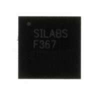
C8051F367-GM Silicon Laboratories Inc, C8051F367-GM Datasheet - Page 186

C8051F367-GM
Manufacturer Part Number
C8051F367-GM
Description
IC 8051 MCU 32K FLASH 28-QFN
Manufacturer
Silicon Laboratories Inc
Series
C8051F36xr
Specifications of C8051F367-GM
Program Memory Type
FLASH
Program Memory Size
32KB (32K x 8)
Package / Case
28-QFN
Core Processor
8051
Core Size
8-Bit
Speed
50MHz
Connectivity
SMBus (2-Wire/I²C), SPI, UART/USART
Peripherals
POR, PWM, Temp Sensor, WDT
Number Of I /o
25
Ram Size
1K x 8
Voltage - Supply (vcc/vdd)
2.7 V ~ 3.6 V
Data Converters
A/D 17x10b; D/A 1x10b
Oscillator Type
Internal
Operating Temperature
-40°C ~ 85°C
Processor Series
C8051F3x
Core
8051
Data Bus Width
8 bit
Data Ram Size
1 KB
Interface Type
I2C/SMBus/SPI/UART
Maximum Clock Frequency
50 MHz
Number Of Programmable I/os
25
Number Of Timers
4
Maximum Operating Temperature
+ 85 C
Mounting Style
SMD/SMT
3rd Party Development Tools
KSK-SL-TOOLSTICK, PK51, CA51, A51, ULINK2
Development Tools By Supplier
C8051F360DK
Minimum Operating Temperature
- 40 C
On-chip Adc
21-ch x 10-bit
On-chip Dac
1-ch x 10-bit
Package
28QFN EP
Device Core
8051
Family Name
C8051F36x
Maximum Speed
50 MHz
Operating Supply Voltage
3 V
Lead Free Status / RoHS Status
Lead free / RoHS Compliant
For Use With
770-1006 - ISP 4PORT FOR SILABS C8051F MCU336-1410 - KIT DEV FOR C8051F360 FAMILY
Eeprom Size
-
Lead Free Status / Rohs Status
Lead free / RoHS Compliant
Other names
336-1649
Available stocks
Company
Part Number
Manufacturer
Quantity
Price
Company:
Part Number:
C8051F367-GM
Manufacturer:
Silicon Labs
Quantity:
135
- Current page: 186 of 288
- Download datasheet (3Mb)
C8051F360/1/2/3/4/5/6/7/8/9
Registers XBR0 and XBR1 are used to assign the digital I/O resources to the physical I/O Port pins. Note
that when the SMBus is selected, the Crossbar assigns both pins associated with the SMBus (SDA and
SCL); when the UART is selected, the Crossbar assigns both pins associated with the UART (TX and RX).
UART0 pin assignments are fixed for bootloading purposes: UART TX0 is always assigned to P0.1
(C8051F360/3) or P0.4 (C8051F361/2/4/5/6/7/8/9); UART RX0 is always assigned to P0.2 (C8051F360/3)
or P0.5 (C8051F361/2/4/5/6/7/8/9). Standard Port I/Os appear contiguously starting at P0.0 after prioritized
functions and skipped pins are assigned.
Important Note: The SPI can be operated in either 3-wire or 4-wire modes, depending on the state of the
NSSMD1-NSSMD0 bits in register SPI0CN. According to the SPI mode, the NSS signal may or may not be
routed to a Port pin.
186
(32- and 28-
PIN I/O
TX0
RX0
TX0
RX0
SCK
MISO
MOSI
NSS*
SDA
SCL
CP0
CP0A
CP1
CP1A
/SYSCLK
CEX0
CEX1
CEX2
CEX3
CEX4
CEX5
ECI
T0
T1
SF Signals
SF Signals
(48-pin)
pin)
Figure 17.4. Crossbar Priority Decoder with Port Pins Skipped
0
0
1
0
2
0
P0SKIP[0:7]
3
0
P0
4
0
5
0
6
0
7
0
0
1
1
1
2
0
P1SKIP[0:7]
3
0
P1
4
0
Rev. 1.0
5
0
6
0
7
0
(32-pin and 28-pin packages)
(48-pin package)
(*4-Wire SPI Only)
0
0
1
0
2
0
P2SKIP[0:7]
3
0
P2
4
0
5
0
6
0
7
0
0
0
32/48-pin only
available on
1
0
P3.1-P3.4
2
0
P3SKIP[0:7]
3
0
P3
4
0
available
P3.5-P3.7
on 48-pin
5
0
only
6
0
7
0
Related parts for C8051F367-GM
Image
Part Number
Description
Manufacturer
Datasheet
Request
R
Part Number:
Description:
SMD/C°/SINGLE-ENDED OUTPUT SILICON OSCILLATOR
Manufacturer:
Silicon Laboratories Inc
Part Number:
Description:
Manufacturer:
Silicon Laboratories Inc
Datasheet:
Part Number:
Description:
N/A N/A/SI4010 AES KEYFOB DEMO WITH LCD RX
Manufacturer:
Silicon Laboratories Inc
Datasheet:
Part Number:
Description:
N/A N/A/SI4010 SIMPLIFIED KEY FOB DEMO WITH LED RX
Manufacturer:
Silicon Laboratories Inc
Datasheet:
Part Number:
Description:
N/A/-40 TO 85 OC/EZLINK MODULE; F930/4432 HIGH BAND (REV E/B1)
Manufacturer:
Silicon Laboratories Inc
Part Number:
Description:
EZLink Module; F930/4432 Low Band (rev e/B1)
Manufacturer:
Silicon Laboratories Inc
Part Number:
Description:
I°/4460 10 DBM RADIO TEST CARD 434 MHZ
Manufacturer:
Silicon Laboratories Inc
Part Number:
Description:
I°/4461 14 DBM RADIO TEST CARD 868 MHZ
Manufacturer:
Silicon Laboratories Inc
Part Number:
Description:
I°/4463 20 DBM RFSWITCH RADIO TEST CARD 460 MHZ
Manufacturer:
Silicon Laboratories Inc
Part Number:
Description:
I°/4463 20 DBM RADIO TEST CARD 868 MHZ
Manufacturer:
Silicon Laboratories Inc
Part Number:
Description:
I°/4463 27 DBM RADIO TEST CARD 868 MHZ
Manufacturer:
Silicon Laboratories Inc
Part Number:
Description:
I°/4463 SKYWORKS 30 DBM RADIO TEST CARD 915 MHZ
Manufacturer:
Silicon Laboratories Inc
Part Number:
Description:
N/A N/A/-40 TO 85 OC/4463 RFMD 30 DBM RADIO TEST CARD 915 MHZ
Manufacturer:
Silicon Laboratories Inc
Part Number:
Description:
I°/4463 20 DBM RADIO TEST CARD 169 MHZ
Manufacturer:
Silicon Laboratories Inc


