MC908MR32CFUE Freescale Semiconductor, MC908MR32CFUE Datasheet - Page 47
MC908MR32CFUE
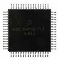
Manufacturer Part Number
MC908MR32CFUE
Description
IC MCU 8MHZ 32K FLASH 64-QFP
Manufacturer
Freescale Semiconductor
Series
HC08r
Datasheet
1.MC908MR16CFUE.pdf
(282 pages)
Specifications of MC908MR32CFUE
Core Processor
HC08
Core Size
8-Bit
Speed
8MHz
Connectivity
SCI, SPI
Peripherals
LVD, POR, PWM
Number Of I /o
44
Program Memory Size
32KB (32K x 8)
Program Memory Type
FLASH
Ram Size
768 x 8
Voltage - Supply (vcc/vdd)
4.5 V ~ 5.5 V
Data Converters
A/D 10x10b
Oscillator Type
Internal
Operating Temperature
-40°C ~ 85°C
Package / Case
64-QFP
Processor Series
HC08MR
Core
HC08
Data Bus Width
8 bit
Data Ram Size
768 B
Interface Type
SCI/SPI
Maximum Clock Frequency
8.2 MHz
Number Of Programmable I/os
44
Number Of Timers
6
Operating Supply Voltage
0 V to 5 V
Maximum Operating Temperature
+ 85 C
Mounting Style
SMD/SMT
Development Tools By Supplier
FSICEBASE, M68CBL05CE
Minimum Operating Temperature
- 40 C
On-chip Adc
10-ch x 10-bit
Lead Free Status / RoHS Status
Lead free / RoHS Compliant
Eeprom Size
-
Lead Free Status / Rohs Status
Lead free / RoHS Compliant
Available stocks
Company
Part Number
Manufacturer
Quantity
Price

Company:
Part Number:
MC908MR32CFUE
Manufacturer:
Freescale Semiconductor
Quantity:
10 000
Part Number:
MC908MR32CFUE
Manufacturer:
NXP/恩智浦
Quantity:
20 000


3.3.1 ADC Port I/O Pins
PTC1/ATD9:PTC0/ATD8 and PTB7/ATD7:PTB0/ATD0 are general-purpose I/O pins that are shared with
the ADC channels.
The channel select bits define which ADC channel/port pin will be used as the input signal. The ADC
overrides the port logic when that port is selected by the ADC multiplexer. The remaining ADC
channels/port pins are controlled by the port logic and can be used as general-purpose input/output (I/O)
pins. Writes to the port register or DDR will not have any effect on the port pin that is selected by the ADC.
Read of a port pin which is in use by the ADC will return a 0.
3.3.2 Voltage Conversion
When the input voltage to the ADC equals V
input voltage equals V
straight-line linear conversions. All other input voltages will result in $3FF if greater than V
if less than V
Freescale Semiconductor
INTERNAL
DATA BUS
REFL
AIEN
Input voltage should not exceed the analog supply voltages. See
19.13 Analog-to-Digital Converter (ADC)
INTERRUPT
LOGIC
.
READ PTB/PTC
COCO
REFL
BUS CLOCK
CONVERSION
MC68HC908MR32 • MC68HC908MR16 Data Sheet, Rev. 6.1
CGMXCLK
COMPLETE
, the ADC converts it to $000. Input voltages between V
Figure 3-2. ADC Block Diagram
ADIV[2:0]
ADC DATA REGISTERS
GENERATOR
REFH
CLOCK
ADC
ADC CLOCK
, the ADC converts the signal to $3FF (full scale). If the
NOTE
ADICLK
Characteristics.
ADC VOLTAGE IN
ADVIN
DISABLE
CHANNEL
SELECT
ADC CHANNEL x
REFH
PTB/Cx
Functional Description
and V
REFH
ADCH[4:0]
REFL
and $000
are
47
Related parts for MC908MR32CFUE
Image
Part Number
Description
Manufacturer
Datasheet
Request
R

Part Number:
Description:
Manufacturer:
Freescale Semiconductor, Inc
Datasheet:
Part Number:
Description:
Manufacturer:
Freescale Semiconductor, Inc
Datasheet:
Part Number:
Description:
Manufacturer:
Freescale Semiconductor, Inc
Datasheet:
Part Number:
Description:
Manufacturer:
Freescale Semiconductor, Inc
Datasheet:
Part Number:
Description:
Manufacturer:
Freescale Semiconductor, Inc
Datasheet:
Part Number:
Description:
Manufacturer:
Freescale Semiconductor, Inc
Datasheet:
Part Number:
Description:
Manufacturer:
Freescale Semiconductor, Inc
Datasheet:
Part Number:
Description:
Manufacturer:
Freescale Semiconductor, Inc
Datasheet:
Part Number:
Description:
Manufacturer:
Freescale Semiconductor, Inc
Datasheet:
Part Number:
Description:
Manufacturer:
Freescale Semiconductor, Inc
Datasheet:
Part Number:
Description:
Manufacturer:
Freescale Semiconductor, Inc
Datasheet:
Part Number:
Description:
Manufacturer:
Freescale Semiconductor, Inc
Datasheet:
Part Number:
Description:
Manufacturer:
Freescale Semiconductor, Inc
Datasheet:
Part Number:
Description:
Manufacturer:
Freescale Semiconductor, Inc
Datasheet:
Part Number:
Description:
Manufacturer:
Freescale Semiconductor, Inc
Datasheet: