D12332VFC20V Renesas Electronics America, D12332VFC20V Datasheet - Page 618
D12332VFC20V
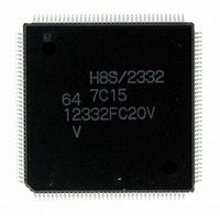
Manufacturer Part Number
D12332VFC20V
Description
IC H8S/2332 MCU ROMLESS 144QFP
Manufacturer
Renesas Electronics America
Series
H8® H8S/2300r
Specifications of D12332VFC20V
Core Processor
H8S/2000
Core Size
16-Bit
Speed
20MHz
Connectivity
SCI, SmartCard
Peripherals
DMA, POR, PWM, WDT
Number Of I /o
106
Program Memory Type
ROMless
Ram Size
8K x 8
Voltage - Supply (vcc/vdd)
2.7 V ~ 3.6 V
Data Converters
A/D 12x10b; D/A 4x8b
Oscillator Type
Internal
Operating Temperature
-20°C ~ 75°C
Package / Case
144-QFP
For Use With
EDK2329 - DEV EVALUATION KIT H8S/2329
Lead Free Status / RoHS Status
Lead free / RoHS Compliant
Eeprom Size
-
Program Memory Size
-
Available stocks
Company
Part Number
Manufacturer
Quantity
Price
Company:

Part Number:
D12332VFC20V
Manufacturer:
Renesas Electronics America
Quantity:
10 000


Bit 5—Reserved: This bit should be written with 0.
Bits 4 to 0—Reserved: These bits cannot be modified and are always read as 1.
13.2.4
The watchdog timer’s TCNT, TCSR, and RSTCSR registers differ from other registers in being
more difficult to write to. The procedures for writing to and reading these registers are given
below.
Writing to TCNT and TCSR: These registers must be written to by a word transfer instruction.
They cannot be written to with byte instructions.
Figure 13.2 shows the format of data written to TCNT and TCSR. TCNT and TCSR both have the
same write address. For a write to TCNT, the upper byte of the written word must contain H'5A
and the lower byte must contain the write data. For a write to TCSR, the upper byte of the written
word must contain H'A5 and the lower byte must contain the write data. This transfers the write
data from the lower byte to TCNT or TCSR.
Writing to RSTCSR: RSTCSR must be written to by a word transfer instruction to address
H'FFBE. It cannot be written to with byte instructions.
Figure 13.3 shows the format of data written to RSTCSR. The method of writing 0 to the WOVF
bit differs from that for writing to the RSTE bit.
To write 0 to the WOVF bit, the write data must have H'A5 in the upper byte and H'00 in the
lower byte. This clears the WOVF bit to 0, but has no effect on the RSTE bit. To write to the
RSTE bit, the upper byte must contain H'5A and the lower byte must contain the write data. This
writes the value in bit 6 of the lower byte into the RSTE bit, but has no effect on the WOVF bit.
Rev.4.00 Sep. 07, 2007 Page 586 of 1210
REJ09B0245-0400
TCNT write
TCSR write
Notes on Register Access
Address: H'FFBC
Address: H'FFBC
Figure 13.2 Writing to TCNT and TCSR
15
15
H'5A
H'A5
8 7
8 7
Write data
Write data
0
0
Related parts for D12332VFC20V
Image
Part Number
Description
Manufacturer
Datasheet
Request
R

Part Number:
Description:
KIT STARTER FOR M16C/29
Manufacturer:
Renesas Electronics America
Datasheet:

Part Number:
Description:
KIT STARTER FOR R8C/2D
Manufacturer:
Renesas Electronics America
Datasheet:

Part Number:
Description:
R0K33062P STARTER KIT
Manufacturer:
Renesas Electronics America
Datasheet:

Part Number:
Description:
KIT STARTER FOR R8C/23 E8A
Manufacturer:
Renesas Electronics America
Datasheet:

Part Number:
Description:
KIT STARTER FOR R8C/25
Manufacturer:
Renesas Electronics America
Datasheet:

Part Number:
Description:
KIT STARTER H8S2456 SHARPE DSPLY
Manufacturer:
Renesas Electronics America
Datasheet:

Part Number:
Description:
KIT STARTER FOR R8C38C
Manufacturer:
Renesas Electronics America
Datasheet:

Part Number:
Description:
KIT STARTER FOR R8C35C
Manufacturer:
Renesas Electronics America
Datasheet:

Part Number:
Description:
KIT STARTER FOR R8CL3AC+LCD APPS
Manufacturer:
Renesas Electronics America
Datasheet:
Part Number:
Description:
KIT STARTER FOR RX610
Manufacturer:
Renesas Electronics America
Datasheet:

Part Number:
Description:
KIT STARTER FOR R32C/118
Manufacturer:
Renesas Electronics America
Datasheet:

Part Number:
Description:
KIT DEV RSK-R8C/26-29
Manufacturer:
Renesas Electronics America
Datasheet:

Part Number:
Description:
KIT STARTER FOR SH7124
Manufacturer:
Renesas Electronics America
Datasheet:

Part Number:
Description:
KIT STARTER FOR H8SX/1622
Manufacturer:
Renesas Electronics America
Datasheet:

Part Number:
Description:
KIT DEV FOR SH7203
Manufacturer:
Renesas Electronics America
Datasheet: