M38513E4FP#U0 Renesas Electronics America, M38513E4FP#U0 Datasheet
M38513E4FP#U0
Specifications of M38513E4FP#U0


Related parts for M38513E4FP#U0


M38513E4FP#U0 Summary of contents
Page 1
To our customers, Old Company Name in Catalogs and Other Documents st On April 1 , 2010, NEC Electronics Corporation merged with Renesas Technology Corporation, and Renesas Electronics Corporation took over all the business of both companies. Therefore, although the ...
Page 2
All information included in this document is current as of the date this document is issued. Such information, however, is subject to change without any prior notice. Before purchasing or using any Renesas Electronics products listed herein, please confirm ...
Page 3
To all our customers Regarding the change of names mentioned in the document, such as Mitsubishi Electric and Mitsubishi XX, to Renesas Technology Corp. The semiconductor operations of Hitachi and Mitsubishi Electric were transferred to Renesas Technology Corporation on April ...
Page 4
This data sheet explains the products which have ROM DESCRIPTION The 3851 group is the 8-bit microcomputer based on the 740 fam- ily core technology. The 3851 group is designed for the household products and office automation equipment ...
Page 5
FUNCTIONAL BLOCK Fig. 2 Functional block diagram 2 MITSUBISHI MICROCOMPUTERS 3851 Group (Built- ROM) SINGLE-CHIP 8-BIT CMOS MICROCOMPUTER ...
Page 6
PIN DESCRIPTION Table 1 Pin description Pin Name Power source CC SS CNV CNV input SS SS Reference V REF voltage input Analog power AVss source input RESET Reset input X Clock input IN X Clock output ...
Page 7
GROUP EXPANSION Mitsubishi plans to expand the 3851 group as follows: Memory Type Support for mask ROM and One Time PROM versions. Memory Size ROM/PROM size ............................................................ 16 K bytes RAM size ......................................................................... 512 bytes Memory Expansion Plan R O ...
Page 8
FUNCTIONAL DESCRIPTION CENTRAL PROCESSING UNIT (CPU) The 3851 group uses the standard 740 Family instruction set. Re- fer to the table of 740 Family addressing modes and machine instructions or the 740 Family Software Manual for details on the instruction ...
Page 9
MEMORY Special Function Register (SFR) Area The Special Function Register area in the zero page contains con- trol registers such as I/O ports and timers. RAM RAM is used for data storage and for stack area of subroutine calls and ...
Page 10
...
Page 11
I/O PORTS The I/O ports have direction registers which determine the input/ output direction of each individual pin. Each bit in a direction reg- ister corresponds to one pin, and each pin can be set to be input port or ...
Page 12
Data bus Port latch ( ...
Page 13
...
Page 14
INTERRUPTS Interrupts occur by 16 sources among 16 sources: seven external, eight internal, and one software. Interrupt Control Each interrupt is controlled by an interrupt request bit, an interrupt enable bit, and the interrupt disable flag except for the software ...
Page 15
Table 3 Interrupt vector addresses and priority Vector Addresses (Note 1) Interrupt Source Priority High 1 FFFD Reset (Note 2) INT 0 2 FFFB SCL, SDA 3 FFF9 INT 1 4 FFF7 5 FFF5 INT 2 INT 3 6 FFF3 ...
Page 16
Interrupt request bit Interrupt enable bit Interrupt disable flag (I) Fig. 9 Interrupt control ...
Page 17
TIMERS The 3851 group has four timers: timer X, timer Y, timer 1, and timer 2. The division ratio of each timer or prescaler is given by 1/(n + 1), where n is the value in the corresponding timer or ...
Page 18
IN f(X )/2 IN Pulse width Timer X count source selection bit measurement mode CNTR active 0 Event edge selection counter P2 /CNTR 7 0 “0” bit mode “1” Port P2 7 Port P2 7 latch direction register ...
Page 19
SERIAL I/O Serial I/O can be used as either clock synchronous or asynchro- nous (UART) serial I/O. A dedicated timer is also provided for baud rate generation CLK BRG count source selection ...
Page 20
Asynchronous Serial I/O (UART) Mode Clock asynchronous serial I/O mode (UART) can be selected by clearing the serial I/O mode selection bit (b6) of the serial I/O con- trol register to “0”. Eight serial data transfer formats can be ...
Page 21
Transmit or receive clock Transmit buffer write signal TBE=0 TSC=0 TBE=1 Serial output Receive buffer read signal ST Serial input Notes 1: Error flag detection occurs at the same time that ...
Page 22
Serial I/O status register (SIOSTS : address 0019 ) 16 Transmit buffer empty flag (TBE) 0: Buffer full 1: Buffer empty Receive buffer full flag (RBF) 0: Buffer empty 1: Buffer full Transmit shift completion flag (TSC) 0: ...
Page 23
MULTI-MASTER I C-BUS INTERFACE 2 The multi-master I C-BUS interface is a serial communications cir- 2 cuit, conforming to the Philips I C-BUS data transfer format. This interface, offering both arbitration lost detection and a synchro ...
Page 24
C Data Shift Register (S0)] 002B 2 The I C data shift register (S0 : address 002B register to store receive data and write transmit data. When transmit data is written into this register transferred to ...
Page 25
C Clock Control Register (S2)] 002F 2 The I C clock control register (address 002F control, SCL mode and SCL frequency. •Bits SCL frequency control bits (CCR0–CCR4) These bits control the SCL frequency. Refer to ...
Page 26
C Control Register (S1D)] 002E 2 The I C control register (address 002E ) controls data communi- 16 cation format. •Bits Bit counter (BC0–BC2) These bits decide the number of bits for the next 1-byte ...
Page 27
C Status Register (S1)] 002D 2 The I C status register (address 002D ) controls the I 16 terface status. The low-order 4 bits are read-only bits and the high-order 4 bits can be read out and written ...
Page 28
Communication mode specification bit (transfer direc- tion specification bit: TRX) This bit decides a direction of transfer for data communication. When this bit is “0,” the reception mode is selected and the data of a transmitting device is ...
Page 29
START Condition Generating Method When writing “1” to the MST, TRX, and BB bits of the I register (address 002D ) at the same time after writing the slave 16 2 address to the I C data shift register (address ...
Page 30
C START/STOP Condition Control Register (S2D)] 0030 16 2 The I C START/STOP condition control register (address 0030 controls START/STOP condition detection. •Bits START/STOP condition set bit (SSC4–SSC0) SCL release time, setup time, and hold ...
Page 31
START/STOP condition SIS SIP SSC4 SSC3 SSC2 SSC1 SSC0 control register (S2D : address 0030 START/STOP condition set bit selection bit 0 : Falling edge active 1 : Rising edge active ...
Page 32
Example of Master Transmission An example of master transmission in the standard clock mode, at the SCL frequency of 100 kHz and in the ACK return mode is shown below. Set a slave address in the high-order 7 bits of ...
Page 33
Precautions when using multi-master I BUS interface (1) Read-modify-write instruction The precautions when the read-modify-write instruction such as SEB, CLB etc. is executed for each register of the multi-master 2 I C-BUS interface are described below. 2 • ...
Page 34
PULSE WIDTH MODULATION (PWM) The 3851 group has a PWM function with an 8-bit resolution, based on a signal that is the clock input X vided by 2. Data Setting The PWM output pin also functions as port P4 riod ...
Page 35
PWM control register (PWMCON : address 001D PWM function enable bit 0: PWM disabled 1: PWM enabled Count source selection bit 0: f f(X )/2 IN Not used (return “0” when read) Fig. 34 Structure ...
Page 36
A-D CONVERTER [A-D Conversion Registers (ADL, ADH)] 0035 , 0036 16 16 The A-D conversion registers are read-only registers that store the result of an A-D conversion. Do not read these registers during an A-D conversion [AD Control Register (ADCON)] ...
Page 37
WATCHDOG TIMER The watchdog timer gives a mean of returning to the reset status when a program cannot run on a normal loop (for example, be- cause of a software run-away). The watchdog timer consists of an 8-bit watchdog timer ...
Page 38
RESET CIRCUIT To reset the microcomputer, RESET pin must be held at an “L” level for 20 cycles or more Then the RESET pin is returned “H” level (the power source voltage must be ...
Page 39
...
Page 40
CLOCK GENERATING CIRCUIT The 3851 group has two built-in oscillation circuits: main clock X -X oscillation circuit and sub clock X IN OUT circuit. An oscillation circuit can be formed by connecting a reso- nator between X and X (X ...
Page 41
MISRG (MISRG : address 0038 Oscillation stabilizing time set after STP instruction released bit 0: Automatically set “01 “FF ” to Prescaler Automatically set nothing Reserved bit “0” Do not write “1“. Not used (return ...
Page 42
“ 1 ” ...
Page 43
NOTES ON PROGRAMMING Processor Status Register The contents of the processor status register (PS) after a reset are undefined, except for the interrupt disable flag (I) which is “1.” Af- ter a reset, initialize flags which affect program execution. In ...
Page 44
DATA REQUIRED FOR MASK ORDERS The following are necessary when ordering a mask ROM produc- tion: 1.Mask ROM Order Confirmation Form 2.Mark Specification Form 3.Data to be written to ROM, in EPROM form (three identical cop- ies) D ATA R ...
Page 45
ELECTRICAL CHARACTERISTICS Table 11 Absolute maximum ratings Symbol Parameter V Power source voltage CC Input voltage P0 – – REF V Input voltage ...
Page 46
Table 13 Recommended operating conditions ( 2 – °C, unless otherwise noted Symbol “H” peak output current I OH(peak) “L” peak output current I OL(peak) I “L” peak output ...
Page 47
Table 14 Electrical characteristics (V = 2 – °C, unless otherwise noted Symbol Parameter “H” output voltage P0 – – ...
Page 48
Table 15 Electrical characteristics (V = 2 – °C, unless otherwise noted Symbol Parameter I Power source current CC SINGLE-CHIP 8-BIT CMOS MICROCOMPUTER Test conditions High-speed ...
Page 49
Table 16 A-D converter characteristics (V = 2 Symbol Parameter – Resolution – Absolute accuracy (excluding quantization error) t Conversion time CONV R Ladder resistor LADDER ...
Page 50
TIMING REQUIREMENTS Table 17 Timing requirements ( 4 – °C, unless otherwise noted Symbol t (RESET) Reset input “L” pulse width ...
Page 51
Table 19 Switching characteristics 4 – °C, unless otherwise noted Symbol Serial I/O clock output “H” pulse width WH CLK ...
Page 52
Measurement output pin CMOS output Fig. 50 Circuit for measuring output switching characteris- tics (1) SINGLE-CHIP 8-BIT CMOS MICROCOMPUTER Measurement output pin 100pF Fig. 51 Circuit for measuring output switching characteris- tics (2) MITSUBISHI MICROCOMPUTERS 3851 Group (Built- ...
Page 53
CNTR , CNTR 0 1 INT to INT 0 3 RESET CLK Fig. 52 Timing diagram 50 SINGLE-CHIP 8-BIT CMOS MICROCOMPUTER t C(CNTR) t WH(CNTR) 0.8V CC 0.2V t WH(INT) 0.8V ...
Page 54
MULTI-MASTER I C-BUS BUS LINE CHARACTERISTICS 2 Table 21 Multi-master I C-BUS bus line characteristics Symbol t Bus free time BUF t Hold time for START condition HD;STA t Hold time for S clock = “0” LOW CL t ...
Page 55
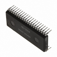
PACKAGE OUTLINE 42P2R-A/E EIAJ Package Code JEDEC Code SSOP42-P-450-0.80 – Detail SINGLE-CHIP 8-BIT CMOS MICROCOMPUTER Weight(g) Lead Material 0.63 Alloy Detail F ...
Page 56
Keep safety first in your circuit designs! • Mitsubishi Electric Corporation puts the maximum effort into making semiconductor products better and more reliable, but there is always the possibility that trouble may occur with them. Trouble with semiconductors may lead ...
Page 57
REVISION HISTORY Rev. Date Page 1.0 05/15/98 First Edition 1.1 07/26/02 Group name is changed. Figure 1 is partly revised. 1 Table 1 is partly added. 3 Figure 3 is partly revised. 4 Figure 6 is partly revised. 7 Figure ...