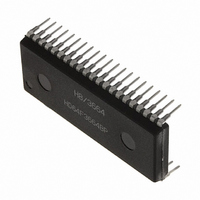
M38513E4FP#U0 Renesas Electronics America, M38513E4FP#U0 Datasheet - Page 43

M38513E4FP#U0
Manufacturer Part Number
M38513E4FP#U0
Description
IC 740 MCU ROM 16K 42SSOP
Manufacturer
Renesas Electronics America
Series
740/38000r
Specifications of M38513E4FP#U0
Core Processor
740
Core Size
8-Bit
Speed
8MHz
Connectivity
SIO, UART/USART
Peripherals
PWM, WDT
Number Of I /o
34
Program Memory Size
16KB (16K x 8)
Program Memory Type
OTP
Ram Size
512 x 8
Voltage - Supply (vcc/vdd)
2.7 V ~ 5.5 V
Data Converters
A/D 5x10b
Oscillator Type
External
Operating Temperature
-20°C ~ 85°C
Package / Case
42-SSOP
Package
42SSOP
Family Name
740
Maximum Speed
8 MHz
Operating Supply Voltage
5 V
Data Bus Width
8 Bit
Number Of Programmable I/os
34
Interface Type
I2C-BUS
On-chip Adc
5-chx10-bit
Number Of Timers
4
Lead Free Status / RoHS Status
Contains lead / RoHS non-compliant
Eeprom Size
-
NOTES ON PROGRAMMING
Processor Status Register
The contents of the processor status register (PS) after a reset are
undefined, except for the interrupt disable flag (I) which is “1.” Af-
ter a reset, initialize flags which affect program execution. In
particular, it is essential to initialize the index X mode (T) and the
decimal mode (D) flags because of their effect on calculations.
Interrupts
The contents of the interrupt request bits do not change immedi-
ately after they have been written. After writing to an interrupt
request register, execute at least one instruction before perform-
ing a BBC or BBS instruction.
Decimal Calculations
• To calculate in decimal notation, set the decimal mode flag (D)
• In decimal mode, the values of the negative (N), overflow (V),
Timers
If a value n (between 0 and 255) is written to a timer latch, the fre-
quency division ratio is 1/(n+1).
Multiplication and Division Instructions
• The index X mode (T) and the decimal mode (D) flags do not af-
• The execution of these instructions does not change the con-
Ports
The contents of the port direction registers cannot be read. The
following cannot be used:
• The data transfer instruction (LDA, etc.)
• The operation instruction when the index X mode flag (T) is “1”
• The addressing mode which uses the value of a direction regis-
• The bit-test instruction (BBC or BBS, etc.) to a direction register
• The read-modify-write instructions (ROR, CLB, or SEB, etc.) to
Use instructions such as LDM and STA, etc., to set the port direc-
tion registers.
Serial I/O
In clock synchronous serial I/O, if the receive side is using an ex-
ternal clock and it is to output the S
enable bit, the receive enable bit, and the S
to “1.”
Serial I/O continues to output the final bit from the T
transmission is completed.
When an external clock is used as synchronous clock in serial I/O,
write transmission data to the transmit buffer register while the
transfer clock is “H.”
40
to “1”, then execute an ADC or SBC instruction. After executing
an ADC or SBC instruction, execute at least one instruction be-
fore executing a SEC, CLC, or CLD instruction.
and zero (Z) flags are invalid.
fect the MUL and DIV instruction.
tents of the processor status register.
ter as an index
a direction register.
RDY
signal, set the transmit
RDY
output enable bit
X
D pin after
A-D Converter
The comparator uses internal capacitors whose charge will be lost
if the clock frequency is too low.
Therefore, make sure that f(X
A-D conversion.
Do not execute the STP instruction during an A-D conversion.
Instruction Execution Time
The instruction execution time is obtained by multiplying the fre-
quency of the internal clock
execute an instruction.
The number of cycles required to execute an instruction is shown
in the list of machine instructions.
The frequency of the internal clock
high-speed mode.
NOTES ON USAGE
Handling of Source Pins
In order to avoid a latch-up occurrence, connect a capacitor suit-
able for high frequencies as bypass capacitor between power
source pin (V
source pin (V
pin). Besides, connect the capacitor to as close as possible. For
bypass capacitor which should not be located too far from the pins
to be connected, a ceramic capacitor of 0.01 F–0.1 F is recom-
mended.
EPROM Version/One Time PROM Version
The CNVss pin is connected to the internal memory circuit block
by a low-ohmic resistance, since it has the multiplexed function to
be a programmable power source pin (V
To improve the noise reduction, connect a track between CNVss
pin and Vss pin or Vcc pin with 1 to 10 k
The mask ROM version track of CNVss pin has no operational in-
terference even if it is connected to Vss pin or Vcc pin via a
resistor.
Electric Characteristic Differences Between
Mask ROM and One Time PROM Version
MCUs
There are differences in electric characteristics, operation margin,
noise immunity, and noise radiation between Mask ROM and One
Time PROM version MCUs due to the differences in the manufac-
turing processes.
When manufacturing an application system with the One Time
PROM version and then switching to use of the Mask ROM ver-
sion, please perform sufficient evaluations for the commercial
samples of the Mask ROM version.
SINGLE-CHIP 8-BIT CMOS MICROCOMPUTER
CC
CC
pin) and GND pin (V
pin) and analog power source input pin (AV
MITSUBISHI MICROCOMPUTERS
IN
by the number of cycles needed to
) is at least on 500 kHz during an
(Built-in 16 KB ROM)
is half of the X
SS
PP
pin) and between power
3851 Group
resistance.
pin) as well.
IN
frequency in
SS


