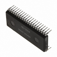
M38513E4FP#U0 Renesas Electronics America, M38513E4FP#U0 Datasheet - Page 29

M38513E4FP#U0
Manufacturer Part Number
M38513E4FP#U0
Description
IC 740 MCU ROM 16K 42SSOP
Manufacturer
Renesas Electronics America
Series
740/38000r
Specifications of M38513E4FP#U0
Core Processor
740
Core Size
8-Bit
Speed
8MHz
Connectivity
SIO, UART/USART
Peripherals
PWM, WDT
Number Of I /o
34
Program Memory Size
16KB (16K x 8)
Program Memory Type
OTP
Ram Size
512 x 8
Voltage - Supply (vcc/vdd)
2.7 V ~ 5.5 V
Data Converters
A/D 5x10b
Oscillator Type
External
Operating Temperature
-20°C ~ 85°C
Package / Case
42-SSOP
Package
42SSOP
Family Name
740
Maximum Speed
8 MHz
Operating Supply Voltage
5 V
Data Bus Width
8 Bit
Number Of Programmable I/os
34
Interface Type
I2C-BUS
On-chip Adc
5-chx10-bit
Number Of Timers
4
Lead Free Status / RoHS Status
Contains lead / RoHS non-compliant
Eeprom Size
-
START Condition Generating Method
When writing “1” to the MST, TRX, and BB bits of the I
register (address 002D
address to the I
condition in which the ES0 bit of the I
002E
that, the bit counter becomes “000
put. The START condition generating timing is different in the
standard clock mode and the high-speed clock mode. Refer to
Figure 26, the START condition generating timing diagram, and
Table 6, the START condition generating timing table.
Fig. 26 START condition generating timing diagram
Note: Absolute time at
STOP Condition Generating Method
When the ES0 bit of the I
“1,” write “1” to the MST and TRX bits, and write “0” to the BB bit
of the I
STOP condition occurs. The STOP condition generating timing is
different in the standard clock mode and the high-speed clock
mode. Refer to Figure 27, the STOP condition generating timing
diagram, and Table 7, the STOP condition generating timing table.
Fig. 27 STOP condition generating timing diagram
Note: Absolute time at
26
Table 6 START condition generating timing table
Table 7 STOP condition generating timing table
I
write signal
S
S
Setup time
Setup time
I
write signal
S
S
2
Hold time
2
Hold time
CL
DA
CL
DA
C status register
C status register
Item
Item
16
number of
number of
2
) and the BB flag are “0”, a START condition occurs. After
C status register (address 002D
2
Standard clock mode
Standard clock mode
cycles.
cycles.
C data shift register (address 002B
5.0 s (20 cycles)
5.0 s (20 cycles)
5.0 s (20 cycles)
4.5 s (18 cycles)
= 4 MHz. The value in parentheses denotes the
= 4 MHz. The value in parentheses denotes the
16
) at the same time after writing the slave
2
Setup
Setup
C control register (address 002E
time
time
2
” and an S
Hold time
Hold time
2
C control register (address
16
High-speed clock mode
High-speed clock mode
2.5 s (10 cycles)
2.5 s (10 cycles)
) simultaneously. Then a
3.0 s (12 cycles)
2.5 s (10 cycles)
CL
for 1 byte is out-
16
) with the
2
C status
16
) is
START/STOP Condition Detecting Operation
The START/STOP condition detection operations are shown in
Figures 28, 29, and Table 8. The START/STOP condition is set by
the START/STOP condition set bit.
The START/STOP condition can be detected only when the input
signal of the S
lease time, setup time, and hold time (see Table 8).
The BB flag is set to “1” by detecting the START condition and is
reset to “0” by detecting the STOP condition.
The BB flag set/reset timing is different in the standard clock mode
and the high-speed clock mode. Refer to Table 8, the BB flag set/
reset time.
Note: When a STOP condition is detected in the slave mode (MST = 0), an
Fig. 28 START condition detecting timing diagram
Fig. 29 STOP condition detecting timing diagram
Table 8 START condition/STOP condition detecting conditions
Note: Unit : Cycle number of system clock
Setup time
BB flag set/
reset time
S
Hold time
CL
S
S
BB flag
release time
S
S
BB flag
interrupt request signal “IICIRQ” occurs to the CPU.
SSC value is the decimal notation value of the START/STOP condi-
tion set bits SSC4 to SSC0. Do not set “0” or an odd number to SSC
value. The value in parentheses is an example when the I
STOP condition control register is set to “18
CL
DA
CL
DA
SINGLE-CHIP 8-BIT CMOS MICROCOMPUTER
CL
SSC value –1
SSC value + 1
SSC value + 1
SSC value + 1 cycle (6.25 s)
and S
Standard clock mode
2
2
2
MITSUBISHI MICROCOMPUTERS
Setup
Setup
time
time
S
S
DA
CL
CL
release time
release time
pins satisfy three conditions: S
cycle < 4.0 s (3.125 s)
cycle < 4.0 s (3.125 s)
+ 2 cycles (3.375 s)
Hold time
Hold time
BB flag
reset
time
(Built-in 16 KB ROM)
BB flag
reset
time
3851 Group
16
” at
High-speed clock mode
4 cycles (1.0 s)
2 cycles (1.0 s)
2 cycles (0.5 s)
3.5 cycles (0.875 s)
= 4 MHz.
2
C START/
CL
re-


