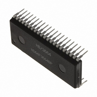
M38513E4FP#U0 Renesas Electronics America, M38513E4FP#U0 Datasheet - Page 25

M38513E4FP#U0
Manufacturer Part Number
M38513E4FP#U0
Description
IC 740 MCU ROM 16K 42SSOP
Manufacturer
Renesas Electronics America
Series
740/38000r
Specifications of M38513E4FP#U0
Core Processor
740
Core Size
8-Bit
Speed
8MHz
Connectivity
SIO, UART/USART
Peripherals
PWM, WDT
Number Of I /o
34
Program Memory Size
16KB (16K x 8)
Program Memory Type
OTP
Ram Size
512 x 8
Voltage - Supply (vcc/vdd)
2.7 V ~ 5.5 V
Data Converters
A/D 5x10b
Oscillator Type
External
Operating Temperature
-20°C ~ 85°C
Package / Case
42-SSOP
Package
42SSOP
Family Name
740
Maximum Speed
8 MHz
Operating Supply Voltage
5 V
Data Bus Width
8 Bit
Number Of Programmable I/os
34
Interface Type
I2C-BUS
On-chip Adc
5-chx10-bit
Number Of Timers
4
Lead Free Status / RoHS Status
Contains lead / RoHS non-compliant
Eeprom Size
-
[I
The I
control, SCL mode and SCL frequency.
•Bits 0 to 4: SCL frequency control bits (CCR0–CCR4)
These bits control the SCL frequency. Refer to Table 5.
•Bit 5: SCL mode specification bit (FAST MODE)
This bit specifies the SCL mode. When this bit is set to “0,” the
standard clock mode is selected. When the bit is set to “1,” the
high-speed clock mode is selected.
When connecting the bus of the high-speed mode I
dard (maximum 400 kbits/s), use 8 MHz or more oscillation
frequency f(X
•Bit 6: ACK bit (ACK BIT)
This bit sets the SDA status when an ACK clock is generated.
When this bit is set to “0,” the ACK return mode is selected and
SDA goes to “L” at the occurrence of an ACK clock. When the bit
is set to “1,” the ACK non-return mode is selected. The SDA is
held in the “H” status at the occurrence of an ACK clock.
However, when the slave address agree with the address data in
the reception of address data at ACK BIT = “0,” the SDA is auto-
matically made “L” (ACK is returned). If there is a disagreement
between the slave address and the address data, the SDA is auto-
matically made “H” (ACK is not returned).
•Bit 7: ACK clock bit (ACK)
This bit specifies the mode of acknowledgment which is an ac-
knowledgment response of data transfer. When this bit is set to
“0,” the no ACK clock mode is selected. In this case, no ACK clock
occurs after data transmission. When the bit is set to “1,” the ACK
clock mode is selected and the master generates an ACK clock
each completion of each 1-byte data transfer. The device for
transmitting address data and control data releases the SDA at
the occurrence of an ACK clock (makes SDA “H”) and receives the
ACK bit generated by the data receiving device.
Note: Do not write data into the I
22
ACK clock: Clock for acknowledgment
2
C Clock Control Register (S2)] 002F
2
data is written during transfer, the I
that data cannot be transferred normally.
C clock control register (address 002F
IN
) and 2 division clock.
2
C clock control register during transfer. If
2
C clock generator is reset, so
16
) is used to set ACK
2
C bus stan-
16
Fig. 21 Structure of I
Table 5 Set values of I
Notes 1: Duty of S
CCR4
0
0
0
0
0
0
0
1
1
1
ACK
b7
Setting value of
CCR3
2: Each value of S
3: The data formula of S
ACK
CCR4–CCR0
BIT
0
0
0
0
0
0
0
1
1
1
only when the high-speed clock mode is selected and CCR value
= 5 (400 kHz, at
from –4 to +2 machine cycles in the standard clock mode, and
fluctuates from –2 to +2 machine cycles in the high-speed clock
mode. In the case of negative fluctuation, the frequency does not
increase because “L” duration is extended instead of “H” duration
reduction.
These are value when S
nous function is not performed. CCR value is the decimal
notation value of the S
more. When using these setting value, use
Do not set 0 to 2 as CCR value regardless of
Set 100 kHz (max.) in the standard clock mode and 400 kHz
(max.) in the high-speed clock mode to the S
ting the S
/(8
/(4
/(2
MODE
SINGLE-CHIP 8-BIT CMOS MICROCOMPUTER
FAST
frequency
CCR2
0
0
0
0
1
1
1
1
1
1
CCR value) Standard clock mode
CCR value) High-speed clock mode (CCR value
CCR value) High-speed clock mode (CCR value = 5)
CCR4 CCR3 CCR2 CCR1 CCR0
CCR1
CL
CL
0
0
1
1
0
0
1
0
1
1
clock output is 50 %. The duty becomes 35 to 45 %
frequency control bits CCR4 to CCR0.
MITSUBISHI MICROCOMPUTERS
2
CCR0
C clock control register
CL
0
1
0
1
0
1
0
1
0
1
= 4 MHz). “H” duration of the clock fluctuates
frequency exceeds the limit at
2
C clock control register and SCL
CL
CL
Setting disabled
Setting disabled
Setting disabled
500/CCR value
Standard clock
CL
frequency is described below:
frequency control bits CCR4 to CCR0.
– (Note 2)
– (Note 2)
clock synchronization by the synchro-
(Note 3)
(Built-in 16 KB ROM)
b0
(at
mode
17.2
16.6
16.1
83.3
100
I
(S2 : address 002F
S
Refer to Table 5.
S
ACK bit
ACK clock bit
SCL frequency
= 4 MHz, unit : kHz)
2
0 : Standard clock mode
1 : High-speed clock mode
0 : ACK is returned.
1 : ACK is not returned.
0 : No ACK clock
1 : ACK clock
C clock control register
CL
CL
3851 Group
frequency control bits
mode specification bit
High-speed clock
1000/CCR value
Setting disabled
Setting disabled
Setting disabled
CL
of 4 MHz or less.
400 (Note 3)
frequency.
frequency by set-
(Note 3)
mode
34.5
33.3
32.3
333
250
166
= 4 MHz or
16
)
5)


