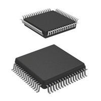
HD6473228F10V Renesas Electronics America, HD6473228F10V Datasheet - Page 130

HD6473228F10V
Manufacturer Part Number
HD6473228F10V
Description
MCU 5V 32K,PB-FREE 64-QFP
Manufacturer
Renesas Electronics America
Series
H8® H8/325r
Datasheet
1.HD6413238F10.pdf
(301 pages)
Specifications of HD6473228F10V
Core Processor
H8/300
Core Size
8-Bit
Speed
10MHz
Connectivity
SCI, UART/USART
Number Of I /o
53
Program Memory Size
8KB (8K x 8)
Program Memory Type
OTP
Ram Size
256 x 8
Voltage - Supply (vcc/vdd)
4.5 V ~ 5.5 V
Oscillator Type
External
Operating Temperature
-20°C ~ 75°C
Package / Case
64-QFP
Lead Free Status / RoHS Status
Lead free / RoHS Compliant
Eeprom Size
-
Data Converters
-
Peripherals
-
Available stocks
Company
Part Number
Manufacturer
Quantity
Price
Company:
Part Number:
HD6473228F10V
Manufacturer:
Renesas Electronics America
Quantity:
10 000
- Current page: 130 of 301
- Download datasheet (2Mb)
1. The sending and receiving H8/325s set their HCSR bits as follows:
2. The sending H8/325 writes the transmit data in the port 3 data register (P3DR). This generates
3. The receiving H8/325 receives the strobe on its input strobe line and latches the data in port 3.
4. The receiving H8/325 reads HCSR, then reads the received data from P3DR. This clears ISF to
5. The input strobe line of the sending H8/325 goes low, setting ISF and generating an input strobe
6. The sending H8/325 reads HCSR, then writes the next transmit data in P3DR. (If it has no next
6.3.5 Interrupts
Regardless of the operating mode or the value of the LTE bit, ISF is always set to 1 when the IS
input changes from high to low. If ISIE is set to 1, an input strobe interrupt (ISI) is requested. In the
software standby mode, LTE must also be set. See section 6.3.3, Operation in Software Standby
Mode.
Sending H8/325:
Receiving H8/325: ISIE = 1, OSE = 1, OSS = 0, LTE = 1, BSE = 0.
an output strobe signal, notifying the receiving H8/325 of data output.
ISF is set to 1, generating an input strobe interrupt.
0 and generates an output strobe signal, notifying the sending H8/325 that the data have been
received.
interrupt.
data to send, it should read P3DR.) This clears ISF to 0 and generates an output strobe signal.
The process now returns to step 3.
Sending H8/325
P3 to P3
Receiving H8/325
OS
IS
H8/325
(sending chip)
7
0
Figure 6-7. Parallel Handshaking Interface Timing Chart (Example)
Write
P3DR
ISIE = 1, OSE = 1, OSS = 1, LTE = 0, BSE = 0.
Interrupt
request
P3DR: Port 3 data register
HCSR: Handshake control/Status register
Read
HCSR
Read
P3DR
121
Interrupt
request
Read
HCSR
Write
P3DR
P3 to P3
IS
OS
H8/325
(receiving chip)
7
Fig 6-7
0
Related parts for HD6473228F10V
Image
Part Number
Description
Manufacturer
Datasheet
Request
R

Part Number:
Description:
KIT STARTER FOR M16C/29
Manufacturer:
Renesas Electronics America
Datasheet:

Part Number:
Description:
KIT STARTER FOR R8C/2D
Manufacturer:
Renesas Electronics America
Datasheet:

Part Number:
Description:
R0K33062P STARTER KIT
Manufacturer:
Renesas Electronics America
Datasheet:

Part Number:
Description:
KIT STARTER FOR R8C/23 E8A
Manufacturer:
Renesas Electronics America
Datasheet:

Part Number:
Description:
KIT STARTER FOR R8C/25
Manufacturer:
Renesas Electronics America
Datasheet:

Part Number:
Description:
KIT STARTER H8S2456 SHARPE DSPLY
Manufacturer:
Renesas Electronics America
Datasheet:

Part Number:
Description:
KIT STARTER FOR R8C38C
Manufacturer:
Renesas Electronics America
Datasheet:

Part Number:
Description:
KIT STARTER FOR R8C35C
Manufacturer:
Renesas Electronics America
Datasheet:

Part Number:
Description:
KIT STARTER FOR R8CL3AC+LCD APPS
Manufacturer:
Renesas Electronics America
Datasheet:

Part Number:
Description:
KIT STARTER FOR RX610
Manufacturer:
Renesas Electronics America
Datasheet:

Part Number:
Description:
KIT STARTER FOR R32C/118
Manufacturer:
Renesas Electronics America
Datasheet:

Part Number:
Description:
KIT DEV RSK-R8C/26-29
Manufacturer:
Renesas Electronics America
Datasheet:

Part Number:
Description:
KIT STARTER FOR SH7124
Manufacturer:
Renesas Electronics America
Datasheet:

Part Number:
Description:
KIT STARTER FOR H8SX/1622
Manufacturer:
Renesas Electronics America
Datasheet:

Part Number:
Description:
KIT DEV FOR SH7203
Manufacturer:
Renesas Electronics America
Datasheet:


